C8051F300-GM Silicon Laboratories Inc, C8051F300-GM Datasheet - Page 6
C8051F300-GM
Manufacturer Part Number
C8051F300-GM
Description
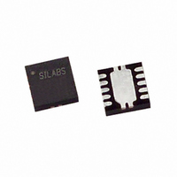
IC 8051 MCU 8K FLASH 11QFN
Manufacturer
Silicon Laboratories Inc
Series
C8051F30xr
Datasheets
1.DTMFDECODER-RD.pdf
(178 pages)
2.C8051F300-TB.pdf
(2 pages)
3.C8051F300-GM.pdf
(174 pages)
Specifications of C8051F300-GM
Program Memory Type
FLASH
Program Memory Size
8KB (8K x 8)
Package / Case
11-VQFN
Core Processor
8051
Core Size
8-Bit
Speed
25MHz
Connectivity
SMBus (2-Wire/I²C), UART/USART
Peripherals
POR, PWM, Temp Sensor, WDT
Number Of I /o
8
Ram Size
256 x 8
Voltage - Supply (vcc/vdd)
2.7 V ~ 3.6 V
Data Converters
A/D 8x8b
Oscillator Type
Internal
Operating Temperature
-40°C ~ 85°C
Processor Series
C8051F3x
Core
8051
Data Bus Width
8 bit
Data Ram Size
256 B
Interface Type
I2C, SMBus, UART
Maximum Clock Frequency
25 MHz
Number Of Programmable I/os
8
Number Of Timers
3 bit
Operating Supply Voltage
2.7 V to 3.6 V
Maximum Operating Temperature
+ 85 C
Mounting Style
SMD/SMT
3rd Party Development Tools
PK51, CA51, A51, ULINK2
Development Tools By Supplier
C8051F226DK
Minimum Operating Temperature
- 40 C
On-chip Adc
8 bit, 8 Channel
No. Of I/o's
8
Ram Memory Size
256Byte
Cpu Speed
25MHz
No. Of Timers
3
Rohs Compliant
Yes
Package
11QFN EP
Device Core
8051
Family Name
C8051F30x
Maximum Speed
25 MHz
Lead Free Status / RoHS Status
Lead free / RoHS Compliant
For Use With
770-1006 - ISP 4PORT FOR SILABS C8051F MCU336-1444 - ADAPTER PROGRAM TOOLSTICK F300336-1351 - KIT REF DES TEMP COMPENS RTC336-1348 - KIT STARTER TOOLSTICK336-1283 - KIT REF DESIGN DTMF DECODER336-1278 - KIT TOOL EVAL SYS IN A USB STICK336-1246 - DEV KIT F300/301/302/303/304/305
Eeprom Size
-
Lead Free Status / Rohs Status
Lead free / RoHS Compliant
Other names
336-1245
Available stocks
Company
Part Number
Manufacturer
Quantity
Price
Company:

Part Number:
C8051F300-GM
Manufacturer:
SiliconL
Quantity:
1 888
Company:
Part Number:
C8051F300-GM
Manufacturer:
TST
Quantity:
5 000
Part Number:
C8051F300-GMR
Manufacturer:
SILICON LABS/èٹ¯ç§‘
Quantity:
20 000


C8051F300/1/2/3/4/5
9. Reset Sources......................................................................................................... 81
10. Flash Memory ......................................................................................................... 87
11. Oscillators ............................................................................................................... 93
12. Port Input/Output.................................................................................................... 99
13. SMBus ................................................................................................................... 107
6
8.4. Power Management Modes .............................................................................. 78
9.1. Power-On Reset ............................................................................................... 82
9.2. Power-Fail Reset / VDD Monitor....................................................................... 82
9.3. External Reset .................................................................................................. 83
9.4. Missing Clock Detector Reset........................................................................... 83
9.5. Comparator0 Reset........................................................................................... 83
9.6. PCA Watchdog Timer Reset............................................................................. 83
9.7. Flash Error Reset.............................................................................................. 84
9.8. Software Reset ................................................................................................. 84
10.1.Programming The Flash Memory ..................................................................... 87
10.2.Non-Volatile Data Storage................................................................................ 88
10.3.Security Options ............................................................................................... 88
11.1.Programmable Internal Oscillator ..................................................................... 93
11.2.External Oscillator Drive Circuit........................................................................ 95
11.3.System Clock Selection.................................................................................... 95
11.4.External Crystal Example ................................................................................. 97
11.5.External RC Example ....................................................................................... 98
11.6.External Capacitor Example ............................................................................. 98
12.1.Priority Crossbar Decoder .............................................................................. 100
12.2.Port I/O Initialization ....................................................................................... 102
12.3.General Purpose Port I/O ............................................................................... 104
13.1.Supporting Documents ................................................................................... 108
13.2.SMBus Configuration...................................................................................... 108
13.3.SMBus Operation ........................................................................................... 108
13.4.Using the SMBus............................................................................................ 111
13.5.SMBus Transfer Modes.................................................................................. 119
8.3.4. Interrupt Latency ...................................................................................... 71
8.3.5. Interrupt Register Descriptions................................................................. 73
8.4.1. Idle Mode.................................................................................................. 78
8.4.2. Stop Mode ................................................................................................ 79
10.1.1.Flash Lock and Key Functions ................................................................. 87
10.1.2.Flash Erase Procedure ............................................................................ 87
10.1.3.Flash Write Procedure ............................................................................. 88
13.3.1.Arbitration............................................................................................... 109
13.3.2.Clock Low Extension.............................................................................. 110
13.3.3.SCL Low Timeout................................................................................... 110
13.3.4.SCL High (SMBus Free) Timeout .......................................................... 110
13.4.1.SMBus Configuration Register............................................................... 112
13.4.2.SMB0CN Control Register ..................................................................... 115
13.4.3.Data Register ......................................................................................... 118
Rev. 2.6
Related parts for C8051F300-GM
Image
Part Number
Description
Manufacturer
Datasheet
Request
R

Part Number:
Description:
SMD/C°/SINGLE-ENDED OUTPUT SILICON OSCILLATOR
Manufacturer:
Silicon Laboratories Inc
Part Number:
Description:
Manufacturer:
Silicon Laboratories Inc
Datasheet:
Part Number:
Description:
N/A N/A/SI4010 AES KEYFOB DEMO WITH LCD RX
Manufacturer:
Silicon Laboratories Inc
Datasheet:
Part Number:
Description:
N/A N/A/SI4010 SIMPLIFIED KEY FOB DEMO WITH LED RX
Manufacturer:
Silicon Laboratories Inc
Datasheet:
Part Number:
Description:
N/A/-40 TO 85 OC/EZLINK MODULE; F930/4432 HIGH BAND (REV E/B1)
Manufacturer:
Silicon Laboratories Inc
Part Number:
Description:
EZLink Module; F930/4432 Low Band (rev e/B1)
Manufacturer:
Silicon Laboratories Inc
Part Number:
Description:
I°/4460 10 DBM RADIO TEST CARD 434 MHZ
Manufacturer:
Silicon Laboratories Inc
Part Number:
Description:
I°/4461 14 DBM RADIO TEST CARD 868 MHZ
Manufacturer:
Silicon Laboratories Inc
Part Number:
Description:
I°/4463 20 DBM RFSWITCH RADIO TEST CARD 460 MHZ
Manufacturer:
Silicon Laboratories Inc
Part Number:
Description:
I°/4463 20 DBM RADIO TEST CARD 868 MHZ
Manufacturer:
Silicon Laboratories Inc
Part Number:
Description:
I°/4463 27 DBM RADIO TEST CARD 868 MHZ
Manufacturer:
Silicon Laboratories Inc
Part Number:
Description:
I°/4463 SKYWORKS 30 DBM RADIO TEST CARD 915 MHZ
Manufacturer:
Silicon Laboratories Inc
Part Number:
Description:
N/A N/A/-40 TO 85 OC/4463 RFMD 30 DBM RADIO TEST CARD 915 MHZ
Manufacturer:
Silicon Laboratories Inc
Part Number:
Description:
I°/4463 20 DBM RADIO TEST CARD 169 MHZ
Manufacturer:
Silicon Laboratories Inc