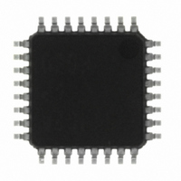
M37544G2AGP#U0 Renesas Electronics America, M37544G2AGP#U0 Datasheet - Page 43

M37544G2AGP#U0
Manufacturer Part Number
M37544G2AGP#U0
Description
IC 740 MCU OTP 8K 32LQFP
Manufacturer
Renesas Electronics America
Series
740/38000r
Specifications of M37544G2AGP#U0
Core Processor
740
Core Size
8-Bit
Speed
8MHz
Connectivity
SIO, UART/USART
Peripherals
WDT
Number Of I /o
25
Program Memory Size
8KB (8K x 8)
Program Memory Type
QzROM
Ram Size
256 x 8
Voltage - Supply (vcc/vdd)
4 V ~ 5.5 V
Data Converters
A/D 6x8b
Oscillator Type
Internal
Operating Temperature
-20°C ~ 85°C
Package / Case
32-LQFP
Lead Free Status / RoHS Status
Lead free / RoHS Compliant
Eeprom Size
-
Available stocks
Company
Part Number
Manufacturer
Quantity
Price
Rev.1.04
REJ03B0012-0104Z
7544 Group
Fig. 49 Selection of packages
(2) Wiring for RESET pin
Make the length of wiring which is connected to the RESET pin as
short as possible. Especially, connect a capacitor across the
RESET pin and the V
(within 20mm).
<Reason>
The width of a pulse input into the RESET pin is determined by the
timing necessary conditions. If noise having a shorter pulse width
than the standard is input to the RESET pin, the reset is released
before the internal state of the microcomputer is completely initial-
ized. This may cause a program runaway.
Fig. 50 Wiring for the RESET pin
NOTES ON USE
Countermeasures against noise
1. Shortest wiring length
(1) Package
Select the smallest possible package to make the total wiring
length short.
<Reason>
The wiring length depends on a microcomputer package. Use of a
small package, for example QFP and not DIP, makes the total wir-
ing length short to reduce influence of noise.
DIP
Reset
circuit
2004.06.08
V
SS
SS
SDIP
pin with the shortest possible wiring
page 41 of 66
Reset
circuit
N.G.
O.K.
Noise
V
SS
SOP
RESET
RESET
V
V
SS
SS
QFP
Fig. 52 Wiring for CNVss pin
(3) Wiring for clock input/output pins
• Make the length of wiring which is connected to clock I/O pins as
• Make the length of wiring (within 20 mm) across the grounding
• Separate the V
<Reason>
If noise enters clock I/O pins, clock waveforms may be deformed.
This may cause a program failure or program runaway. Also, if a
potential difference is caused by the noise between the V
of a microcomputer and the V
clock will not be input in the microcomputer.
Fig. 51 Wiring for clock I/O pins
(4) Wiring to CNVss pin
Connect the CNVss pin to the Vss pin with the shortest possible
wiring.
<Reason>
The processor mode of a microcomputer is influenced by a poten-
tial at the CNVss pin. If a potential difference is caused by the
noise between pins CNVss and Vss, the processor mode may be-
come unstable. This may cause a microcomputer malfunction or a
program runaway.
short as possible.
lead of a capacitor which is connected to an oscillator and the
V
terns.
SS
pin of a microcomputer as short as possible.
CNV
V
SS
SS
N.G.
N.G.
SS
Noise
pattern only for oscillation from other V
Noise
X
X
V
IN
OUT
SS
SS
level of an oscillator, the correct
CNV
O.K.
O.K.
X
X
V
V
IN
OUT
SS
SS
SS
SS
SS
level
pat-


