R5F21244SNFP#U0 Renesas Electronics America, R5F21244SNFP#U0 Datasheet - Page 276
R5F21244SNFP#U0
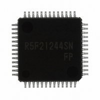
Manufacturer Part Number
R5F21244SNFP#U0
Description
IC R8C MCU FLASH 16K 52LQFP
Manufacturer
Renesas Electronics America
Series
M16C™ M16C/R8C/Tiny/24r
Datasheets
1.R5F211A2SPU0.pdf
(300 pages)
2.R5F21246SDFPU0.pdf
(61 pages)
3.R5F21246SDFPU0.pdf
(527 pages)
Specifications of R5F21244SNFP#U0
Core Processor
R8C
Core Size
16-Bit
Speed
20MHz
Connectivity
I²C, LIN, SIO, SSU, UART/USART
Peripherals
POR, Voltage Detect, WDT
Number Of I /o
41
Program Memory Size
16KB (16K x 8)
Program Memory Type
FLASH
Ram Size
1K x 8
Voltage - Supply (vcc/vdd)
2.2 V ~ 5.5 V
Data Converters
A/D 12x10b
Oscillator Type
Internal
Operating Temperature
-20°C ~ 85°C
Package / Case
52-LQFP
For Use With
R0K521256S000BE - KIT EVAL STARTER FOR R8C/25
Lead Free Status / RoHS Status
Lead free / RoHS Compliant
Eeprom Size
-
Available stocks
Company
Part Number
Manufacturer
Quantity
Price

Part Number:
R5F21244SNFP#U0R5F21244SNFP#V2
Manufacturer:
Renesas Electronics America
Quantity:
10 000


R8C/24 Group, R8C/25 Group
Rev.3.00
REJ09B0244-0300
Figure 14.103 Registers TRDSR0 to TRDSR1 in PWM3 Mode
Timer RD Status Register i (i = 0 or 1)
b7 b6 b5 b4 b3
NOTES:
1.
2.
The w riting results are as follow s:
• This bit is set to 0 w hen the read result is 1 and 0 is w ritten to the same bit.
• This bit remains unchanged even if the read result is 0 and 0 is w ritten to the same bit (this bit remains
• This bit remains unchanged if 1 is w ritten to it.
Including w hen the BFji (j = C or D) bit in the TRDMR register is set to 1 (TRDGRji is used as the buffer register).
Feb 29, 2008
1 even if it is set to 1 from 0 after reading, and w riting 0).
b2
b1 b0
Bit Symbol
TRDSR0
TRDSR1
(b7-b6)
Symbol
IMFA
IMFB
IMFC
IMFD
OVF
UDF
Page 257 of 485
—
Input capture/compare match flag A
Input capture/compare match flag B
Input capture/compare match flag C
Input capture/compare match flag D
Overflow flag
Underflow flag
Nothing is assigned. If necessary, set to 0.
When read, the content is 1.
Address
Bit Name
(1)
0143h
0153h
[Source for setting this bit to 0]
Write 0 after read
[Source for setting this bit to 1]
When the value in the TRDi register
matches w ith the value in the TRDGRAi
register.
[Source for setting this bit to 0]
Write 0 after read
[Source for setting this bit to 1]
When the value in the TRDi register
matches w ith the value in the TRDGRBi
register.
[Source for setting this bit to 0]
Write 0 after read
[Source for setting this bit to 1]
When the value in the TRDi register
matches w ith the value in the TRDGRCi
register
[Source for setting this bit to 0]
Write 0 after read
[Source for setting this bit to 1]
When the value in the TRDi register
matches w ith the value in the TRDGRDi
register
[Source for setting this bit to 0]
Write 0 after read
[Source for setting this bit to 1]
When the TRDi register overflow s.
This bit is disabled in PWM3 mode.
(2)
(2)
.
.
After Reset
11100000b
11000000b
Function
(1)
(1)
(1)
(1)
(1)
.
.
.
.
.
14. Timers
RW
RW
RW
RW
RW
RW
RW
—
Related parts for R5F21244SNFP#U0
Image
Part Number
Description
Manufacturer
Datasheet
Request
R

Part Number:
Description:
KIT STARTER FOR M16C/29
Manufacturer:
Renesas Electronics America
Datasheet:

Part Number:
Description:
KIT STARTER FOR R8C/2D
Manufacturer:
Renesas Electronics America
Datasheet:

Part Number:
Description:
R0K33062P STARTER KIT
Manufacturer:
Renesas Electronics America
Datasheet:

Part Number:
Description:
KIT STARTER FOR R8C/23 E8A
Manufacturer:
Renesas Electronics America
Datasheet:

Part Number:
Description:
KIT STARTER FOR R8C/25
Manufacturer:
Renesas Electronics America
Datasheet:

Part Number:
Description:
KIT STARTER H8S2456 SHARPE DSPLY
Manufacturer:
Renesas Electronics America
Datasheet:

Part Number:
Description:
KIT STARTER FOR R8C38C
Manufacturer:
Renesas Electronics America
Datasheet:

Part Number:
Description:
KIT STARTER FOR R8C35C
Manufacturer:
Renesas Electronics America
Datasheet:

Part Number:
Description:
KIT STARTER FOR R8CL3AC+LCD APPS
Manufacturer:
Renesas Electronics America
Datasheet:
Part Number:
Description:
KIT STARTER FOR RX610
Manufacturer:
Renesas Electronics America
Datasheet:

Part Number:
Description:
KIT STARTER FOR R32C/118
Manufacturer:
Renesas Electronics America
Datasheet:

Part Number:
Description:
KIT DEV RSK-R8C/26-29
Manufacturer:
Renesas Electronics America
Datasheet:

Part Number:
Description:
KIT STARTER FOR SH7124
Manufacturer:
Renesas Electronics America
Datasheet:

Part Number:
Description:
KIT STARTER FOR H8SX/1622
Manufacturer:
Renesas Electronics America
Datasheet:

Part Number:
Description:
KIT DEV FOR SH7203
Manufacturer:
Renesas Electronics America
Datasheet: