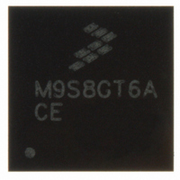
MC9S08GT60CFDE Freescale Semiconductor, MC9S08GT60CFDE Datasheet - Page 180

MC9S08GT60CFDE
Manufacturer Part Number
MC9S08GT60CFDE
Description
IC MCU 60K FLASH 20MHZ 48-QFN
Manufacturer
Freescale Semiconductor
Series
HCS08r
Datasheet
1.M68EVB908GB60E.pdf
(290 pages)
Specifications of MC9S08GT60CFDE
Core Processor
HCS08
Core Size
8-Bit
Speed
40MHz
Connectivity
I²C, SCI, SPI
Peripherals
LVD, POR, PWM, WDT
Number Of I /o
39
Program Memory Size
60KB (60K x 8)
Program Memory Type
FLASH
Ram Size
4K x 8
Voltage - Supply (vcc/vdd)
1.8 V ~ 3.6 V
Data Converters
A/D 8x10b
Oscillator Type
Internal
Operating Temperature
-40°C ~ 85°C
Package / Case
48-QFN
For Use With
M68DEMO908GB60E - BOARD DEMO MC9S08GB60M68EVB908GB60E - BOARD EVAL FOR MC9S08GB60
Lead Free Status / RoHS Status
Lead free / RoHS Compliant
Eeprom Size
-
Available stocks
Company
Part Number
Manufacturer
Quantity
Price
Company:
Part Number:
MC9S08GT60CFDE
Manufacturer:
ON
Quantity:
130
Company:
Part Number:
MC9S08GT60CFDE
Manufacturer:
FREESCALE
Quantity:
1 831
Part Number:
MC9S08GT60CFDE
Manufacturer:
FREESCALE
Quantity:
20 000
- Current page: 180 of 290
- Download datasheet (2Mb)
Serial Communications Interface (SCI) Module
11.10.3 SCI x Control Register 2 (SCIxC2)
This register can be read or written at any time.
TIE — Transmit Interrupt Enable (for TDRE)
TCIE — Transmission Complete Interrupt Enable (for TC)
RIE — Receiver Interrupt Enable (for RDRF)
ILIE — Idle Line Interrupt Enable (for IDLE)
TE — Transmitter Enable
180
TE must be 1 in order to use the SCI transmitter. Normally, when TE = 1, the SCI forces the TxD1 pin
to act as an output for the SCI system. If LOOPS = 1 and RSRC = 0, the TxD1 pin reverts to being a
port B general-purpose I/O pin even if TE = 1.
When the SCI is configured for single-wire operation (LOOPS = RSRC = 1), TXDIR controls the
direction of traffic on the single SCI communication line (TxD1 pin).
TE also can be used to queue an idle character by writing TE = 0 then TE = 1 while a transmission is
in progress. Refer to
When TE is written to 0, the transmitter keeps control of the port TxD1 pin until any data, queued idle,
or queued break character finishes transmitting before allowing the pin to revert to a general-purpose
I/O pin.
1 = Hardware interrupt requested when TDRE flag is 1.
0 = Hardware interrupts from TDRE disabled (use polling).
1 = Hardware interrupt requested when TC flag is 1.
0 = Hardware interrupts from TC disabled (use polling).
1 = Hardware interrupt requested when RDRF flag is 1.
0 = Hardware interrupts from RDRF disabled (use polling).
1 = Hardware interrupt requested when IDLE flag is 1.
0 = Hardware interrupts from IDLE disabled (use polling).
1 = Transmitter on.
0 = Transmitter off.
Reset:
Read:
Write:
Section 11.5.2, “Send Break and Queued
Bit 7
TIE
Figure 11-8. SCI x Control Register 2 (SCIxC2)
0
MC9S08GB/GT Data Sheet, Rev. 2.3
TCIE
6
0
RIE
5
0
ILIE
4
0
TE
Idle,”
3
0
for more details.
RE
2
0
RWU
Freescale Semiconductor
1
0
Bit 0
SBK
0
Related parts for MC9S08GT60CFDE
Image
Part Number
Description
Manufacturer
Datasheet
Request
R
Part Number:
Description:
Manufacturer:
Freescale Semiconductor, Inc
Datasheet:
Part Number:
Description:
Manufacturer:
Freescale Semiconductor, Inc
Datasheet:
Part Number:
Description:
Manufacturer:
Freescale Semiconductor, Inc
Datasheet:
Part Number:
Description:
Manufacturer:
Freescale Semiconductor, Inc
Datasheet:
Part Number:
Description:
Manufacturer:
Freescale Semiconductor, Inc
Datasheet:
Part Number:
Description:
Manufacturer:
Freescale Semiconductor, Inc
Datasheet:
Part Number:
Description:
Manufacturer:
Freescale Semiconductor, Inc
Datasheet:
Part Number:
Description:
Manufacturer:
Freescale Semiconductor, Inc
Datasheet:
Part Number:
Description:
Manufacturer:
Freescale Semiconductor, Inc
Datasheet:
Part Number:
Description:
Manufacturer:
Freescale Semiconductor, Inc
Datasheet:
Part Number:
Description:
Manufacturer:
Freescale Semiconductor, Inc
Datasheet:
Part Number:
Description:
Manufacturer:
Freescale Semiconductor, Inc
Datasheet:
Part Number:
Description:
Manufacturer:
Freescale Semiconductor, Inc
Datasheet:
Part Number:
Description:
Manufacturer:
Freescale Semiconductor, Inc
Datasheet:
Part Number:
Description:
Manufacturer:
Freescale Semiconductor, Inc
Datasheet:


