MC9S12C32CFAE25 Freescale Semiconductor, MC9S12C32CFAE25 Datasheet - Page 132
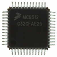
MC9S12C32CFAE25
Manufacturer Part Number
MC9S12C32CFAE25
Description
IC MCU 32K FLASH 25MHZ 48-LQFP
Manufacturer
Freescale Semiconductor
Series
HCS12r
Datasheets
1.MC9S12GC16MFUE.pdf
(690 pages)
2.MC9S12C96CFUER.pdf
(26 pages)
3.MC9S12C32CFAE25.pdf
(2 pages)
4.MC9S12C32CPBE25.pdf
(36 pages)
Specifications of MC9S12C32CFAE25
Core Processor
HCS12
Core Size
16-Bit
Speed
25MHz
Connectivity
CAN, EBI/EMI, SCI, SPI
Peripherals
POR, PWM, WDT
Number Of I /o
31
Program Memory Size
32KB (32K x 8)
Program Memory Type
FLASH
Ram Size
2K x 8
Voltage - Supply (vcc/vdd)
2.35 V ~ 5.5 V
Data Converters
A/D 8x10b
Oscillator Type
Internal
Operating Temperature
-40°C ~ 85°C
Package / Case
48-LQFP
Processor Series
S12C
Core
HCS12
Data Bus Width
16 bit
Data Ram Size
2 KB
Interface Type
CAN/SCI/SPI
Maximum Clock Frequency
25 MHz
Number Of Programmable I/os
31
Number Of Timers
8
Maximum Operating Temperature
+ 85 C
Mounting Style
SMD/SMT
3rd Party Development Tools
EWHCS12
Development Tools By Supplier
M68EVB912C32EE
Minimum Operating Temperature
- 40 C
On-chip Adc
8-ch x 10-bit
For Use With
CML12C32SLK - KIT STUDENT LEARNING 16BIT HCS12
Lead Free Status / RoHS Status
Lead free / RoHS Compliant
Eeprom Size
-
Lead Free Status / Rohs Status
Lead free / RoHS Compliant
Available stocks
Company
Part Number
Manufacturer
Quantity
Price
Company:

Part Number:
MC9S12C32CFAE25
Manufacturer:
FREESCAL
Quantity:
240
Company:
Part Number:
MC9S12C32CFAE25
Manufacturer:
Freescale Semiconductor
Quantity:
10 000


Chapter 4 Multiplexed External Bus Interface (MEBIV3)
132
BKGD/MODC/
TAGHI
PA7/A15/D15/D7
thru
PA0/A8/D8/D0
PB7/A7/D7
thru
PB0/A0/D0
PE7/NOACC
PE6/IPIPE1/
MODB/CLKTO
PE5/IPIPE0/MODA
.
Pin Name
MODC
BKGD
TAGHI
PA7–PA0
A15–A8
D15–D8
D15/D7
thru
D8/D0
PB7–PB0
A7–A0
D7–D0
PE7
NOACC
MODB
PE6
IPIPE1
CLKTO
MODA
PE5
IPIPE0
Pin Functions
Table 4-1. External System Pins Associated With MEBI
MC9S12C-Family / MC9S12GC-Family
At the rising edge on RESET, the state of this pin is registered into the MODC
bit to set the mode. (This pin always has an internal pullup.)
Pseudo open-drain communication pin for the single-wire background debug
mode. There is an internal pull-up resistor on this pin.
When instruction tagging is on, a 0 at the falling edge of E tags the high half of
the instruction word being read into the instruction queue.
General-purpose I/O pins, see PORTA and DDRA registers.
High-order address lines multiplexed during ECLK low. Outputs except in
special peripheral mode where they are inputs from an external tester system.
High-order bidirectional data lines multiplexed during ECLK high in expanded
wide modes, special peripheral mode, and visible internal accesses (IVIS = 1)
in emulation expanded narrow mode. Direction of data transfer is generally
indicated by R/W.
Alternate high-order and low-order bytes of the bidirectional data lines
multiplexed during ECLK high in expanded narrow modes and narrow accesses
in wide modes. Direction of data transfer is generally indicated by R/W.
General-purpose I/O pins, see PORTB and DDRB registers.
Low-order address lines multiplexed during ECLK low. Outputs except in
special peripheral mode where they are inputs from an external tester system.
Low-order bidirectional data lines multiplexed during ECLK high in expanded
wide modes, special peripheral mode, and visible internal accesses (with
IVIS = 1) in emulation expanded narrow mode. Direction of data transfer is
generally indicated by R/W.
General-purpose I/O pin, see PORTE and DDRE registers.
CPU No Access output. Indicates whether the current cycle is a free cycle. Only
available in expanded modes.
At the rising edge of RESET, the state of this pin is registered into the MODB
bit to set the mode.
General-purpose I/O pin, see PORTE and DDRE registers.
Instruction pipe status bit 1, enabled by PIPOE bit in PEAR.
System clock test output. Only available in special modes. PIPOE = 1 overrides
this function. The enable for this function is in the clock module.
At the rising edge on RESET, the state of this pin is registered into the MODA
bit to set the mode.
General-purpose I/O pin, see PORTE and DDRE registers.
Instruction pipe status bit 0, enabled by PIPOE bit in PEAR.
Rev 01.24
Description
Freescale Semiconductor
Related parts for MC9S12C32CFAE25
Image
Part Number
Description
Manufacturer
Datasheet
Request
R

Part Number:
Description:
Manufacturer:
Freescale Semiconductor, Inc
Datasheet:
Part Number:
Description:
Manufacturer:
Freescale Semiconductor, Inc
Datasheet:
Part Number:
Description:
Manufacturer:
Freescale Semiconductor, Inc
Datasheet:
Part Number:
Description:
Manufacturer:
Freescale Semiconductor, Inc
Datasheet:
Part Number:
Description:
Manufacturer:
Freescale Semiconductor, Inc
Datasheet:
Part Number:
Description:
Manufacturer:
Freescale Semiconductor, Inc
Datasheet:
Part Number:
Description:
Manufacturer:
Freescale Semiconductor, Inc
Datasheet:
Part Number:
Description:
Manufacturer:
Freescale Semiconductor, Inc
Datasheet:
Part Number:
Description:
Manufacturer:
Freescale Semiconductor, Inc
Datasheet:
Part Number:
Description:
Manufacturer:
Freescale Semiconductor, Inc
Datasheet:
Part Number:
Description:
Manufacturer:
Freescale Semiconductor, Inc
Datasheet:
Part Number:
Description:
Manufacturer:
Freescale Semiconductor, Inc
Datasheet:
Part Number:
Description:
Manufacturer:
Freescale Semiconductor, Inc
Datasheet:
Part Number:
Description:
Manufacturer:
Freescale Semiconductor, Inc
Datasheet:
Part Number:
Description:
Manufacturer:
Freescale Semiconductor, Inc
Datasheet: