MC9S12C32CFAE25 Freescale Semiconductor, MC9S12C32CFAE25 Datasheet - Page 356
MC9S12C32CFAE25
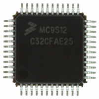
Manufacturer Part Number
MC9S12C32CFAE25
Description
IC MCU 32K FLASH 25MHZ 48-LQFP
Manufacturer
Freescale Semiconductor
Series
HCS12r
Datasheets
1.MC9S12GC16MFUE.pdf
(690 pages)
2.MC9S12C96CFUER.pdf
(26 pages)
3.MC9S12C32CFAE25.pdf
(2 pages)
4.MC9S12C32CPBE25.pdf
(36 pages)
Specifications of MC9S12C32CFAE25
Core Processor
HCS12
Core Size
16-Bit
Speed
25MHz
Connectivity
CAN, EBI/EMI, SCI, SPI
Peripherals
POR, PWM, WDT
Number Of I /o
31
Program Memory Size
32KB (32K x 8)
Program Memory Type
FLASH
Ram Size
2K x 8
Voltage - Supply (vcc/vdd)
2.35 V ~ 5.5 V
Data Converters
A/D 8x10b
Oscillator Type
Internal
Operating Temperature
-40°C ~ 85°C
Package / Case
48-LQFP
Processor Series
S12C
Core
HCS12
Data Bus Width
16 bit
Data Ram Size
2 KB
Interface Type
CAN/SCI/SPI
Maximum Clock Frequency
25 MHz
Number Of Programmable I/os
31
Number Of Timers
8
Maximum Operating Temperature
+ 85 C
Mounting Style
SMD/SMT
3rd Party Development Tools
EWHCS12
Development Tools By Supplier
M68EVB912C32EE
Minimum Operating Temperature
- 40 C
On-chip Adc
8-ch x 10-bit
For Use With
CML12C32SLK - KIT STUDENT LEARNING 16BIT HCS12
Lead Free Status / RoHS Status
Lead free / RoHS Compliant
Eeprom Size
-
Lead Free Status / Rohs Status
Lead free / RoHS Compliant
Available stocks
Company
Part Number
Manufacturer
Quantity
Price
Company:

Part Number:
MC9S12C32CFAE25
Manufacturer:
FREESCAL
Quantity:
240
Company:
Part Number:
MC9S12C32CFAE25
Manufacturer:
Freescale Semiconductor
Quantity:
10 000


Chapter 12 Pulse-Width Modulator (PWM8B6CV1) Block Description
12.3.2.4
This register selects the prescale clock source for clocks A and B independently.
Read: anytime
Write: anytime
356
Module Base + 0x0003
PCLK5
PCLK4
PCLK3
PCLK2
PCLK1
PCLK0
Reset
Field
5
4
3
2
1
0
W
R
Pulse Width Channel 5 Clock Select
0 Clock A is the clock source for PWM channel 5.
1 Clock SA is the clock source for PWM channel 5.
Pulse Width Channel 4 Clock Select
0 Clock A is the clock source for PWM channel 4.
1 Clock SA is the clock source for PWM channel 4.
Pulse Width Channel 3 Clock Select
0 Clock B is the clock source for PWM channel 3.
1 Clock SB is the clock source for PWM channel 3.
Pulse Width Channel 2 Clock Select
0 Clock B is the clock source for PWM channel 2.
1 Clock SB is the clock source for PWM channel 2.
Pulse Width Channel 1 Clock Select
0 Clock A is the clock source for PWM channel 1.
1 Clock SA is the clock source for PWM channel 1.
Pulse Width Channel 0 Clock Select
0 Clock A is the clock source for PWM channel 0.
1 Clock SA is the clock source for PWM channel 0.
PWM Prescale Clock Select Register (PWMPRCLK)
0
0
7
PCKB2–PCKB0 and PCKA2–PCKA0 register bits can be written anytime.
If the clock prescale is changed while a PWM signal is being generated, a
truncated or stretched pulse can occur during the transition.
Figure 12-6. PWM Prescaler Clock Select Register (PWMPRCLK)
= Unimplemented or Reserved
PCKB2
0
6
Table 12-4. PWMCLK Field Descriptions
PCKB1
MC9S12C-Family / MC9S12GC-Family
0
5
PCKB0
Rev 01.24
NOTE
0
4
Description
0
0
3
PCKA2
0
2
PCKA1
Freescale Semiconductor
0
1
PCKA0
0
0
Related parts for MC9S12C32CFAE25
Image
Part Number
Description
Manufacturer
Datasheet
Request
R

Part Number:
Description:
Manufacturer:
Freescale Semiconductor, Inc
Datasheet:
Part Number:
Description:
Manufacturer:
Freescale Semiconductor, Inc
Datasheet:
Part Number:
Description:
Manufacturer:
Freescale Semiconductor, Inc
Datasheet:
Part Number:
Description:
Manufacturer:
Freescale Semiconductor, Inc
Datasheet:
Part Number:
Description:
Manufacturer:
Freescale Semiconductor, Inc
Datasheet:
Part Number:
Description:
Manufacturer:
Freescale Semiconductor, Inc
Datasheet:
Part Number:
Description:
Manufacturer:
Freescale Semiconductor, Inc
Datasheet:
Part Number:
Description:
Manufacturer:
Freescale Semiconductor, Inc
Datasheet:
Part Number:
Description:
Manufacturer:
Freescale Semiconductor, Inc
Datasheet:
Part Number:
Description:
Manufacturer:
Freescale Semiconductor, Inc
Datasheet:
Part Number:
Description:
Manufacturer:
Freescale Semiconductor, Inc
Datasheet:
Part Number:
Description:
Manufacturer:
Freescale Semiconductor, Inc
Datasheet:
Part Number:
Description:
Manufacturer:
Freescale Semiconductor, Inc
Datasheet:
Part Number:
Description:
Manufacturer:
Freescale Semiconductor, Inc
Datasheet:
Part Number:
Description:
Manufacturer:
Freescale Semiconductor, Inc
Datasheet: