MC908AP64CFAE Freescale Semiconductor, MC908AP64CFAE Datasheet - Page 15
MC908AP64CFAE
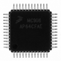
Manufacturer Part Number
MC908AP64CFAE
Description
IC MCU 64K 8MHZ SPI 48-LQFP
Manufacturer
Freescale Semiconductor
Series
HC08r
Specifications of MC908AP64CFAE
Core Processor
HC08
Core Size
8-Bit
Speed
8MHz
Connectivity
I²C, IRSCI, SCI, SPI
Peripherals
LED, LVD, POR, PWM
Number Of I /o
32
Program Memory Size
64KB (64K x 8)
Program Memory Type
FLASH
Ram Size
2K x 8
Voltage - Supply (vcc/vdd)
2.7 V ~ 5.5 V
Data Converters
A/D 8x10b
Oscillator Type
Internal
Operating Temperature
-40°C ~ 85°C
Package / Case
48-LQFP
Cpu Family
HC08
Device Core Size
8b
Frequency (max)
8MHz
Interface Type
SCI/SPI
Total Internal Ram Size
2KB
# I/os (max)
32
Number Of Timers - General Purpose
4
Operating Supply Voltage (typ)
3.3/5V
Operating Supply Voltage (max)
5.5V
Operating Supply Voltage (min)
2.7V
On-chip Adc
8-chx10-bit
Instruction Set Architecture
CISC
Operating Temp Range
-40C to 85C
Operating Temperature Classification
Industrial
Mounting
Surface Mount
Pin Count
48
Package Type
LQFP
Controller Family/series
HC08
No. Of I/o's
32
Ram Memory Size
2KB
Cpu Speed
8MHz
No. Of Timers
2
Embedded Interface Type
I2C, SCI, SPI
Rohs Compliant
Yes
Processor Series
HC08AP
Core
HC08
Data Bus Width
8 bit
Data Ram Size
2 KB
Maximum Clock Frequency
8 MHz
Number Of Programmable I/os
32
Number Of Timers
4
Maximum Operating Temperature
+ 85 C
Mounting Style
SMD/SMT
Development Tools By Supplier
FSICEBASE, DEMO908AP64E, M68CBL05CE
Minimum Operating Temperature
- 40 C
Package
48LQFP
Family Name
HC08
Maximum Speed
8 MHz
Operating Supply Voltage
3.3|5 V
Lead Free Status / RoHS Status
Lead free / RoHS Compliant
Eeprom Size
-
Lead Free Status / Rohs Status
Compliant
Available stocks
Company
Part Number
Manufacturer
Quantity
Price
Company:

Part Number:
MC908AP64CFAE
Manufacturer:
Freescale
Quantity:
3 359
Company:
Part Number:
MC908AP64CFAE
Manufacturer:
Freescale Semiconductor
Quantity:
10 000
Company:
Part Number:
MC908AP64CFAER
Manufacturer:
Freescale Semiconductor
Quantity:
10 000


15.3
15.3.1
15.3.2
15.3.3
15.3.4
15.3.5
15.3.6
15.3.7
15.3.8
15.4
15.5
15.5.1
15.5.2
15.6
15.6.1
15.6.2
15.6.3
15.6.4
15.6.5
15.7
15.7.1
15.7.2
15.7.3
15.7.4
15.7.5
16.1
16.2
16.2.1
16.2.2
16.2.3
16.3
16.3.1
16.3.2
16.4
16.4.1
16.4.2
16.5
16.5.1
16.5.2
17.1
17.2
Freescale Semiconductor
Functional Description . . . . . . . . . . . . . . . . . . . . . . . . . . . . . . . . . . . . . . . . . . . . . . . . . . . . . . . 248
Interrupts . . . . . . . . . . . . . . . . . . . . . . . . . . . . . . . . . . . . . . . . . . . . . . . . . . . . . . . . . . . . . . . . . 251
Low-Power Modes . . . . . . . . . . . . . . . . . . . . . . . . . . . . . . . . . . . . . . . . . . . . . . . . . . . . . . . . . . 251
I/O Signals . . . . . . . . . . . . . . . . . . . . . . . . . . . . . . . . . . . . . . . . . . . . . . . . . . . . . . . . . . . . . . . . 252
I/O Registers . . . . . . . . . . . . . . . . . . . . . . . . . . . . . . . . . . . . . . . . . . . . . . . . . . . . . . . . . . . . . . 253
Introduction . . . . . . . . . . . . . . . . . . . . . . . . . . . . . . . . . . . . . . . . . . . . . . . . . . . . . . . . . . . . . . . 259
Port A . . . . . . . . . . . . . . . . . . . . . . . . . . . . . . . . . . . . . . . . . . . . . . . . . . . . . . . . . . . . . . . . . . . . 261
Port B . . . . . . . . . . . . . . . . . . . . . . . . . . . . . . . . . . . . . . . . . . . . . . . . . . . . . . . . . . . . . . . . . . . . 263
Port C . . . . . . . . . . . . . . . . . . . . . . . . . . . . . . . . . . . . . . . . . . . . . . . . . . . . . . . . . . . . . . . . . . . . 265
Port D . . . . . . . . . . . . . . . . . . . . . . . . . . . . . . . . . . . . . . . . . . . . . . . . . . . . . . . . . . . . . . . . . . . . 267
Introduction . . . . . . . . . . . . . . . . . . . . . . . . . . . . . . . . . . . . . . . . . . . . . . . . . . . . . . . . . . . . . . . 271
Features . . . . . . . . . . . . . . . . . . . . . . . . . . . . . . . . . . . . . . . . . . . . . . . . . . . . . . . . . . . . . . . . . . 271
ADC Port I/O Pins . . . . . . . . . . . . . . . . . . . . . . . . . . . . . . . . . . . . . . . . . . . . . . . . . . . . . . . 248
Voltage Conversion . . . . . . . . . . . . . . . . . . . . . . . . . . . . . . . . . . . . . . . . . . . . . . . . . . . . . . 248
Conversion Time . . . . . . . . . . . . . . . . . . . . . . . . . . . . . . . . . . . . . . . . . . . . . . . . . . . . . . . . 249
Continuous Conversion . . . . . . . . . . . . . . . . . . . . . . . . . . . . . . . . . . . . . . . . . . . . . . . . . . . 250
Auto-Scan Mode . . . . . . . . . . . . . . . . . . . . . . . . . . . . . . . . . . . . . . . . . . . . . . . . . . . . . . . . 250
Result Justification . . . . . . . . . . . . . . . . . . . . . . . . . . . . . . . . . . . . . . . . . . . . . . . . . . . . . . . 251
Data Register Interlocking . . . . . . . . . . . . . . . . . . . . . . . . . . . . . . . . . . . . . . . . . . . . . . . . . 251
Monotonicity . . . . . . . . . . . . . . . . . . . . . . . . . . . . . . . . . . . . . . . . . . . . . . . . . . . . . . . . . . . . 251
Wait Mode . . . . . . . . . . . . . . . . . . . . . . . . . . . . . . . . . . . . . . . . . . . . . . . . . . . . . . . . . . . . . 252
Stop Mode . . . . . . . . . . . . . . . . . . . . . . . . . . . . . . . . . . . . . . . . . . . . . . . . . . . . . . . . . . . . . 252
ADC Voltage In (V
ADC Analog Power Pin (V
ADC Analog Ground Pin (V
ADC Voltage Reference High Pin (V
ADC Voltage Reference Low Pin (V
ADC Status and Control Register . . . . . . . . . . . . . . . . . . . . . . . . . . . . . . . . . . . . . . . . . . . 253
ADC Clock Control Register. . . . . . . . . . . . . . . . . . . . . . . . . . . . . . . . . . . . . . . . . . . . . . . . 254
ADC Data Register 0 (ADRH0 and ADRL0) . . . . . . . . . . . . . . . . . . . . . . . . . . . . . . . . . . . 255
ADC Auto-Scan Mode Data Registers (ADRL1–ADRL3) . . . . . . . . . . . . . . . . . . . . . . . . . 257
ADC Auto-Scan Control Register (ADASCR) . . . . . . . . . . . . . . . . . . . . . . . . . . . . . . . . . . 257
Port A Data Register (PTA) . . . . . . . . . . . . . . . . . . . . . . . . . . . . . . . . . . . . . . . . . . . . . . . . 261
Data Direction Register (DDRA) . . . . . . . . . . . . . . . . . . . . . . . . . . . . . . . . . . . . . . . . . . . . 261
Port-A LED Control Register (LEDA) . . . . . . . . . . . . . . . . . . . . . . . . . . . . . . . . . . . . . . . . . 263
Port B Data Register (PTB) . . . . . . . . . . . . . . . . . . . . . . . . . . . . . . . . . . . . . . . . . . . . . . . . 263
Data Direction Register B (DDRB) . . . . . . . . . . . . . . . . . . . . . . . . . . . . . . . . . . . . . . . . . . . 264
Port C Data Register (PTC) . . . . . . . . . . . . . . . . . . . . . . . . . . . . . . . . . . . . . . . . . . . . . . . . 265
Data Direction Register C (DDRC). . . . . . . . . . . . . . . . . . . . . . . . . . . . . . . . . . . . . . . . . . . 266
Port D Data Register (PTD) . . . . . . . . . . . . . . . . . . . . . . . . . . . . . . . . . . . . . . . . . . . . . . . . 267
Data Direction Register D (DDRD). . . . . . . . . . . . . . . . . . . . . . . . . . . . . . . . . . . . . . . . . . . 268
ADIN
MC68HC908AP Family Data Sheet, Rev. 4
) . . . . . . . . . . . . . . . . . . . . . . . . . . . . . . . . . . . . . . . . . . . . . . . . . . . 252
DDA
Input/Output (I/O) Ports
External Interrupt (IRQ)
SSA
) . . . . . . . . . . . . . . . . . . . . . . . . . . . . . . . . . . . . . . . . . . . . . 252
). . . . . . . . . . . . . . . . . . . . . . . . . . . . . . . . . . . . . . . . . . . . . 252
Chapter 16
Chapter 17
REFL
REFH
) . . . . . . . . . . . . . . . . . . . . . . . . . . . . . . . . . . . . . 252
). . . . . . . . . . . . . . . . . . . . . . . . . . . . . . . . . . . . . 252
15
Related parts for MC908AP64CFAE
Image
Part Number
Description
Manufacturer
Datasheet
Request
R

Part Number:
Description:
Manufacturer:
Freescale Semiconductor, Inc
Datasheet:
Part Number:
Description:
Manufacturer:
Freescale Semiconductor, Inc
Datasheet:
Part Number:
Description:
Manufacturer:
Freescale Semiconductor, Inc
Datasheet:
Part Number:
Description:
Manufacturer:
Freescale Semiconductor, Inc
Datasheet:
Part Number:
Description:
Manufacturer:
Freescale Semiconductor, Inc
Datasheet:
Part Number:
Description:
Manufacturer:
Freescale Semiconductor, Inc
Datasheet:
Part Number:
Description:
Manufacturer:
Freescale Semiconductor, Inc
Datasheet:
Part Number:
Description:
Manufacturer:
Freescale Semiconductor, Inc
Datasheet:
Part Number:
Description:
Manufacturer:
Freescale Semiconductor, Inc
Datasheet:
Part Number:
Description:
Manufacturer:
Freescale Semiconductor, Inc
Datasheet:
Part Number:
Description:
Manufacturer:
Freescale Semiconductor, Inc
Datasheet:
Part Number:
Description:
Manufacturer:
Freescale Semiconductor, Inc
Datasheet:
Part Number:
Description:
Manufacturer:
Freescale Semiconductor, Inc
Datasheet:
Part Number:
Description:
Manufacturer:
Freescale Semiconductor, Inc
Datasheet:
Part Number:
Description:
Manufacturer:
Freescale Semiconductor, Inc
Datasheet: