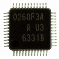
M30260F3AGP#U3A Renesas Electronics America, M30260F3AGP#U3A Datasheet - Page 263

M30260F3AGP#U3A
Manufacturer Part Number
M30260F3AGP#U3A
Description
IC M16C/26A MCU FLASH 24K 48LQFP
Manufacturer
Renesas Electronics America
Series
M16C™ M16C/Tiny/26r
Specifications of M30260F3AGP#U3A
Core Processor
M16C/60
Core Size
16-Bit
Speed
20MHz
Connectivity
I²C, IEBus, SIO, UART/USART
Peripherals
DMA, PWM, Voltage Detect, WDT
Number Of I /o
39
Program Memory Size
24KB (24K x 8)
Program Memory Type
FLASH
Ram Size
1K x 8
Voltage - Supply (vcc/vdd)
2.7 V ~ 5.5 V
Data Converters
A/D 12x10b
Oscillator Type
Internal
Operating Temperature
-40°C ~ 85°C
Package / Case
48-LQFP
Package
48LQFP
Family Name
R8C
Maximum Speed
20 MHz
Operating Supply Voltage
3.3|5 V
Data Bus Width
16 Bit
Number Of Programmable I/os
39
Interface Type
UART
On-chip Adc
12-chx10-bit
Number Of Timers
8
For Use With
R0K33026AS000BE - KIT DEV EVALUATION M16C/26A
Lead Free Status / RoHS Status
Lead free / RoHS Compliant
Eeprom Size
-
Available stocks
Company
Part Number
Manufacturer
Quantity
Price
- Current page: 263 of 354
- Download datasheet (4Mb)
M
R
R
e
E
1
. v
J
6
Figure 17.5.1.3. Processing Before and After Low Power Dissipation Mode
0
C
2
9
0 .
2 /
B
0
0
6
NOTES:
Jump to the low power consumption mode
program transferred to internal RAM area.
(In the following steps, use the low-power
consumption mode program or internal RAM area)
2
Transfer a low power internal consumption mode
A
0
F
1. Set the FMRSTP bit to “1” after setting the FMR01 bit to “1”(CPU rewrite mode).
2. Wait until the clock stabilizes to switch the clock source of the CPU clock to the main clock or the sub clock.
3. Add a t
2
e
G
0 -
b
o r
1 .
2
0
u
, 5
0
p
2
(
PS
0
M
0
program to RAM area
1
7
wait time by a program. Do not access the flash memory during this wait time.
6
C
page 244
2 /
6
, A
M
1
f o
6
C
3
2
2 /
9
6
, B
M
1
6
C
2 /
6
) T
Low power consumption
Start main clock oscillation
Set the FMSTP bit to “1” (flash memory stopped.
Low power consumption state)
Wait until the flash memory circuit stabilizes (t
Set the FMSTP bit to “0” (flash memory operation)
Process of low power consumption mode or
on-chip oscillator low power consumption mode
switch the clock source of the CPU clock
mode program
Jump to a desired address in the flash memory
Set the FMR01 bit to “1” after setting “0”
(CPU rewrite mode enabled)
Switch the clock source of CPU clock.
Turn main clock off.
(CPU rewrite mode disabled)
Set the FMR01 bit to “0”
(2)
wait until oscillation stabilizes
(1)
17. Flash Memory Version
(2)
PS) (3)
Related parts for M30260F3AGP#U3A
Image
Part Number
Description
Manufacturer
Datasheet
Request
R

Part Number:
Description:
KIT STARTER FOR M16C/29
Manufacturer:
Renesas Electronics America
Datasheet:

Part Number:
Description:
KIT STARTER FOR R8C/2D
Manufacturer:
Renesas Electronics America
Datasheet:

Part Number:
Description:
R0K33062P STARTER KIT
Manufacturer:
Renesas Electronics America
Datasheet:

Part Number:
Description:
KIT STARTER FOR R8C/23 E8A
Manufacturer:
Renesas Electronics America
Datasheet:

Part Number:
Description:
KIT STARTER FOR R8C/25
Manufacturer:
Renesas Electronics America
Datasheet:

Part Number:
Description:
KIT STARTER H8S2456 SHARPE DSPLY
Manufacturer:
Renesas Electronics America
Datasheet:

Part Number:
Description:
KIT STARTER FOR R8C38C
Manufacturer:
Renesas Electronics America
Datasheet:

Part Number:
Description:
KIT STARTER FOR R8C35C
Manufacturer:
Renesas Electronics America
Datasheet:

Part Number:
Description:
KIT STARTER FOR R8CL3AC+LCD APPS
Manufacturer:
Renesas Electronics America
Datasheet:

Part Number:
Description:
KIT STARTER FOR RX610
Manufacturer:
Renesas Electronics America
Datasheet:

Part Number:
Description:
KIT STARTER FOR R32C/118
Manufacturer:
Renesas Electronics America
Datasheet:

Part Number:
Description:
KIT DEV RSK-R8C/26-29
Manufacturer:
Renesas Electronics America
Datasheet:

Part Number:
Description:
KIT STARTER FOR SH7124
Manufacturer:
Renesas Electronics America
Datasheet:

Part Number:
Description:
KIT STARTER FOR H8SX/1622
Manufacturer:
Renesas Electronics America
Datasheet:

Part Number:
Description:
KIT DEV FOR SH7203
Manufacturer:
Renesas Electronics America
Datasheet:


