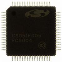
C8051F005-GQ Silicon Laboratories Inc, C8051F005-GQ Datasheet - Page 108

C8051F005-GQ
Manufacturer Part Number
C8051F005-GQ
Description
IC 8051 MCU 32K FLASH 64TQFP
Manufacturer
Silicon Laboratories Inc
Series
C8051F00xr
Specifications of C8051F005-GQ
Program Memory Type
FLASH
Program Memory Size
32KB (32K x 8)
Package / Case
64-TQFP, 64-VQFP
Core Processor
8051
Core Size
8-Bit
Speed
25MHz
Connectivity
SMBus (2-Wire/I²C), SPI, UART/USART
Peripherals
Brown-out Detect/Reset, POR, PWM, Temp Sensor, WDT
Number Of I /o
32
Ram Size
2.25K x 8
Voltage - Supply (vcc/vdd)
2.7 V ~ 3.6 V
Data Converters
A/D 8x12b, D/A 2x12b
Oscillator Type
Internal
Operating Temperature
-40°C ~ 85°C
Processor Series
C8051F0x
Core
8051
Data Bus Width
8 bit
Data Ram Size
2.25 KB
Interface Type
I2C/SMBus/SPI/UART
Maximum Clock Frequency
25 MHz
Number Of Programmable I/os
32
Number Of Timers
4
Operating Supply Voltage
2.7 V to 3.6 V
Maximum Operating Temperature
+ 85 C
Mounting Style
SMD/SMT
3rd Party Development Tools
PK51, CA51, A51, ULINK2
Development Tools By Supplier
C8051F005DK
Minimum Operating Temperature
- 40 C
On-chip Adc
8-ch x 12-bit
On-chip Dac
2-ch x 12-bit
No. Of I/o's
32
Ram Memory Size
2304Byte
Cpu Speed
25MHz
No. Of Timers
4
No. Of Pwm Channels
5
Rohs Compliant
Yes
Lead Free Status / RoHS Status
Lead free / RoHS Compliant
For Use With
336-1188 - DEV KIT FOR F005/006/007
Eeprom Size
-
Lead Free Status / Rohs Status
Lead free / RoHS Compliant
Other names
336-1187
Available stocks
Company
Part Number
Manufacturer
Quantity
Price
Company:
Part Number:
C8051F005-GQ
Manufacturer:
SiliconL
Quantity:
3 141
Company:
Part Number:
C8051F005-GQ
Manufacturer:
Silicon Laboratories Inc
Quantity:
10 000
Company:
Part Number:
C8051F005-GQR
Manufacturer:
AD
Quantity:
8 720
Company:
Part Number:
C8051F005-GQR
Manufacturer:
SIGNALS
Quantity:
20
Company:
Part Number:
C8051F005-GQR
Manufacturer:
Silicon Laboratories Inc
Quantity:
10 000
Part Number:
C8051F005-GQR
Manufacturer:
SILICON LABS/èٹ¯ç§‘
Quantity:
20 000
WEAKPUD
Bit7:
Bit6:
Bits5-1: UNUSED. Read = 00000b, Write = don’t care.
Bit0:
Example Usage of XBR0, XBR1, XBR2:
When selected, the digital resources fill the Port I/O pins in order (top to bottom as shown in
Table 15.1) starting with P0.0 through P0.7, and then P1.0 through P1.7, and finally P2.0
through P2.7. If the digital resources are not mapped to the Port I/O pins, they default to their
matching internal Port Register bits.
Example1: If XBR0 = 0x11, XBR1 = 0x00, and XBR2 = 0x40:
P0.0=SDA, P0.1=SCL, P0.2=CEX0, P0.3=CEX1, P0.4 … P2.7 map to corresponding Port I/O.
Example2: If XBR0 = 0x80, XBR1 = 0x04, and XBR2 = 0x41:
P0.0=CP0, P0.1=/INT0, P0.2 = CNVSTR, P0.3 … P2.7 map to corresponding Port I/O.
R/W
Bit7
0: Weak Pull-ups Enabled (except for Ports whose I/O are configured as push-pull)
1: Weak Pull-ups Disabled
0: Crossbar Disabled
1: Crossbar Enabled
CNVSTE: ADC Convert Start Input Enable Bit
0: CNVSTR unavailable at Port pin.
1: CNVSTR routed to Port Pin.
WEAKPUD: Port I/O Weak Pull-up Disable Bit
XBARE: Crossbar Enable Bit
XBARE
R/W
Bit6
Figure 15.5. XBR2: Port I/O CrossBar Register 2
R/W
Bit5
-
R/W
Bit4
-
Rev. 1.7
R/W
Bit3
-
R/W
Bit2
-
C8051F000/1/2/5/6/7
C8051F010/1/2/5/6/7
R/W
Bit1
-
CNVSTE
R/W
Bit0
SFR Address:
Reset Value
00000000
0xE3
108


