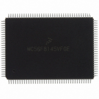
MC56F8145VFGE Freescale Semiconductor, MC56F8145VFGE Datasheet - Page 34

MC56F8145VFGE
Manufacturer Part Number
MC56F8145VFGE
Description
IC DSP 16BIT 40MHZ 128-LQFP
Manufacturer
Freescale Semiconductor
Series
56F8xxxr
Datasheet
1.MC56F8145VFGE.pdf
(172 pages)
Specifications of MC56F8145VFGE
Core Processor
56800
Core Size
16-Bit
Speed
40MHz
Connectivity
EBI/EMI, SCI, SPI
Peripherals
POR, PWM, WDT
Number Of I /o
49
Program Memory Size
128KB (64K x 16)
Program Memory Type
FLASH
Ram Size
4K x 16
Voltage - Supply (vcc/vdd)
2.25 V ~ 3.6 V
Data Converters
A/D 16x12b
Oscillator Type
External
Operating Temperature
-40°C ~ 105°C
Package / Case
128-LQFP
Data Bus Width
16 bit
Processor Series
MC56F81xx
Core
56800E
Data Ram Size
4 KB
Interface Type
SCI, SPI
Maximum Clock Frequency
40 MHz
Number Of Programmable I/os
49
Number Of Timers
8
Maximum Operating Temperature
+ 105 C
Mounting Style
SMD/SMT
Minimum Operating Temperature
- 40 C
On-chip Adc
4 x 12 bit, 4 Channel
Lead Free Status / RoHS Status
Lead free / RoHS Compliant
Eeprom Size
-
Lead Free Status / Rohs Status
Lead free / RoHS Compliant
Available stocks
Company
Part Number
Manufacturer
Quantity
Price
Company:
Part Number:
MC56F8145VFGE
Manufacturer:
Freescale
Quantity:
5
Company:
Part Number:
MC56F8145VFGE
Manufacturer:
Freescale Semiconductor
Quantity:
10 000
Part Number:
MC56F8145VFGE
Manufacturer:
FREESCALE
Quantity:
20 000
34
(GPIOE10)
(GPIOE11)
(GPIOE12)
(GPIOE13)
(GPIOE8)
(GPIOE9)
CAN_TX
Signal
Name
IRQA
IRQB
TC0
TC1
TD0
TD1
TD2
TD3
Table 2-2 Signal and Package Information for the 128-Pin LQFP
Pin No.
120
111
113
107
108
109
110
52
53
Schmitt
Schmitt
Schmitt
Schmitt
Schmitt
Output
Output
Output
Output
Output
Input/
Input/
Input/
Input/
Open
Drain
Type
Input
56F8345 Technical Data, Rev. 17
enabled
enabled
enabled
During
Output
pull-up
pull-up
pull-up
Reset
Input,
Input,
Input,
State
Open
Drain
FlexCAN Transmit Data — CAN output with internal pull-up
enable at reset.*
* Note: If a pin is configured as open drain output mode, internal
pull-up will automatically be disabled when it outputs low.
Internal pull-up will be enabled unless it has been manually
disabled by clearing the corresponding bit in the PUREN register
of the GPIO module, when it outputs high.
If a pin is configured as push-pull output mode, internal pull-up
will automatically be disabled, whether it outputs low or high.
TC0 - 1 — Timer C, Channels 0 and 1
Port E GPIO — These GPIO pins can be individually
programmed as input or output pins.
At reset, these pins default to Timer functionality.
To deactivate the internal pull-up resistor, clear the appropriate
bit of the GPIOE_PUR register. See
TD0 - TD3 — Timer D, Channels 0, 1, 2 and 3
Port E GPIO — These GPIO pins can be individually
programmed as input or output pins.
At reset, these pins default to Timer functionality.
To deactivate the internal pull-up resistor, clear the appropriate
bit of the GPIOE_PUR register. See
External Interrupt Request A and B — The IRQA and IRQB
inputs are asynchronous external interrupt requests during Stop
and Wait mode operation. During other operating modes, they
are synchronized external interrupt requests, which indicate an
external device is requesting service. They can be programmed
to be level-sensitive or negative-edge triggered.
To deactivate the internal pull-up resistor, set the IRQ bit in the
SIM_PUDR register. See
Signal Description
Part 6.5.6
for details.
Part 6.5.6
Part 6.5.6
Freescale Semiconductor
for details.
for details.
Preliminary


