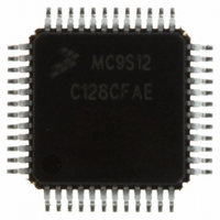
MC9S12C128CFAE Freescale Semiconductor, MC9S12C128CFAE Datasheet - Page 366

MC9S12C128CFAE
Manufacturer Part Number
MC9S12C128CFAE
Description
IC MCU 16BIT 4K FLASH 48-LQFP
Manufacturer
Freescale Semiconductor
Series
HCS12r
Specifications of MC9S12C128CFAE
Core Processor
HCS12
Core Size
16-Bit
Speed
25MHz
Connectivity
CAN, EBI/EMI, SCI, SPI
Peripherals
POR, PWM, WDT
Number Of I /o
31
Program Memory Size
128KB (128K x 8)
Program Memory Type
FLASH
Ram Size
4K x 8
Voltage - Supply (vcc/vdd)
2.35 V ~ 5.5 V
Data Converters
A/D 8x10b
Oscillator Type
Internal
Operating Temperature
-40°C ~ 85°C
Package / Case
48-LQFP
Processor Series
S12C
Core
HCS12
Data Bus Width
16 bit
Data Ram Size
4 KB
Interface Type
CAN/SCI/SPI
Maximum Clock Frequency
25 MHz
Number Of Programmable I/os
31
Number Of Timers
8
Maximum Operating Temperature
+ 85 C
Mounting Style
SMD/SMT
3rd Party Development Tools
EWHCS12
Development Tools By Supplier
M68EVB912C32EE
Minimum Operating Temperature
- 40 C
On-chip Adc
8-ch x 10-bit
Lead Free Status / RoHS Status
Lead free / RoHS Compliant
Eeprom Size
-
Lead Free Status / Rohs Status
Lead free / RoHS Compliant
Available stocks
Company
Part Number
Manufacturer
Quantity
Price
Company:
Part Number:
MC9S12C128CFAE
Manufacturer:
Freescale Semiconductor
Quantity:
10 000
- Current page: 366 of 690
- Download datasheet (4Mb)
Chapter 12 Pulse-Width Modulator (PWM8B6CV1) Block Description
In this way, the output of the PWM will always be either the old waveform or the new waveform, not some
variation in between. If the channel is not enabled, then writes to the period register will go directly to the
latches as well as the buffer.
Reference
To calculate the output period, take the selected clock source period for the channel of interest (A, B, SA,
or SB) and multiply it by the value in the period register for that channel:
For boundary case programming values, please refer to
366
Module Base + 0x0012
Module Base + 0x0013
Module Base + 0x0014
Reset
Reset
Reset
•
•
•
•
W
W
W
R
R
R
The channel is disabled
Left aligned output (CAEx = 0)
PWMx period = channel clock period * PWMPERx center aligned output (CAEx = 1)
PWMx period = channel clock period * (2 * PWMPERx)
Section 12.4.2.3, “PWM Period and Duty,”
Bit 7
Bit 7
Bit 7
0
0
0
7
7
7
Reads of this register return the most recent value written. Reads do not
necessarily return the value of the currently active period due to the double
buffering scheme.
Figure 12-21. PWM Channel Period Registers (PWMPER0)
Figure 12-22. PWM Channel Period Registers (PWMPER1)
Figure 12-23. PWM Channel Period Registers (PWMPER2)
6
0
6
0
6
0
6
6
6
MC9S12C-Family / MC9S12GC-Family
5
0
5
0
5
0
5
5
5
Rev 01.24
NOTE
4
0
4
0
4
0
4
4
4
for more information.
Section 12.4.2.8, “PWM Boundary Cases.”
3
0
3
0
3
0
3
3
3
2
0
2
0
2
0
2
2
2
Freescale Semiconductor
1
0
1
0
1
0
1
1
1
Bit 0
Bit 0
Bit 0
0
0
0
0
0
0
Related parts for MC9S12C128CFAE
Image
Part Number
Description
Manufacturer
Datasheet
Request
R
Part Number:
Description:
Manufacturer:
Freescale Semiconductor, Inc
Datasheet:
Part Number:
Description:
Manufacturer:
Freescale Semiconductor, Inc
Datasheet:
Part Number:
Description:
Manufacturer:
Freescale Semiconductor, Inc
Datasheet:
Part Number:
Description:
Manufacturer:
Freescale Semiconductor, Inc
Datasheet:
Part Number:
Description:
Manufacturer:
Freescale Semiconductor, Inc
Datasheet:
Part Number:
Description:
Manufacturer:
Freescale Semiconductor, Inc
Datasheet:
Part Number:
Description:
Manufacturer:
Freescale Semiconductor, Inc
Datasheet:
Part Number:
Description:
Manufacturer:
Freescale Semiconductor, Inc
Datasheet:
Part Number:
Description:
Manufacturer:
Freescale Semiconductor, Inc
Datasheet:
Part Number:
Description:
Manufacturer:
Freescale Semiconductor, Inc
Datasheet:
Part Number:
Description:
Manufacturer:
Freescale Semiconductor, Inc
Datasheet:
Part Number:
Description:
Manufacturer:
Freescale Semiconductor, Inc
Datasheet:
Part Number:
Description:
Manufacturer:
Freescale Semiconductor, Inc
Datasheet:
Part Number:
Description:
Manufacturer:
Freescale Semiconductor, Inc
Datasheet:
Part Number:
Description:
Manufacturer:
Freescale Semiconductor, Inc
Datasheet:


