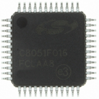
C8051F061-GQ Silicon Laboratories Inc, C8051F061-GQ Datasheet - Page 40

C8051F061-GQ
Manufacturer Part Number
C8051F061-GQ
Description
IC 8051 MCU 64K FLASH 64TQFP
Manufacturer
Silicon Laboratories Inc
Series
C8051F06xr
Specifications of C8051F061-GQ
Program Memory Type
FLASH
Program Memory Size
64KB (64K x 8)
Package / Case
64-TQFP, 64-VQFP
Core Processor
8051
Core Size
8-Bit
Speed
25MHz
Connectivity
CAN, SMBus (2-Wire/I²C), SPI, UART/USART
Peripherals
Brown-out Detect/Reset, POR, PWM, Temp Sensor, WDT
Number Of I /o
24
Ram Size
4.25K x 8
Voltage - Supply (vcc/vdd)
2.7 V ~ 3.6 V
Data Converters
A/D 2x16b, 8x10b; D/A 2x12b
Oscillator Type
Internal
Operating Temperature
-40°C ~ 85°C
Processor Series
C8051F0x
Core
8051
Data Bus Width
8 bit
Data Ram Size
4.25 KB
Interface Type
CAN/I2C/SMBus/SPI/UART
Maximum Clock Frequency
25 MHz
Number Of Programmable I/os
24
Number Of Timers
5
Operating Supply Voltage
2.7 V to 3.6 V
Maximum Operating Temperature
+ 85 C
Mounting Style
SMD/SMT
3rd Party Development Tools
PK51, CA51, A51, ULINK2
Development Tools By Supplier
C8051F060DK
Minimum Operating Temperature
- 40 C
On-chip Adc
2-ch x 16-bit
On-chip Dac
2-ch x 12-bit
Lead Free Status / RoHS Status
Lead free / RoHS Compliant
Eeprom Size
-
Lead Free Status / Rohs Status
Lead free / RoHS Compliant
Other names
336-1215
Available stocks
Company
Part Number
Manufacturer
Quantity
Price
Company:
Part Number:
C8051F061-GQ
Manufacturer:
Silicon Laboratories Inc
Quantity:
10 000
Company:
Part Number:
C8051F061-GQR
Manufacturer:
SILICON
Quantity:
2 100
Company:
Part Number:
C8051F061-GQR
Manufacturer:
Silicon Laboratories Inc
Quantity:
10 000
- Current page: 40 of 328
- Download datasheet (2Mb)
C8051F060/1/2/3/4/5/6/7
40
CNVSTR0
CNVSTR1
VRGND0
VRGND1
VBGAP0
VBGAP1
VREFD
CANTX
CANRX
VREF1
VREF2
AIN0G
AIN1G
Name
DAC0
DAC1
AIN0
AIN1
P0.0
P0.1
P0.2
P0.3
P0.4
F060
F062
20
22
18
19
15
12
94
95
25
62
61
60
59
58
6
7
5
2
3
9
8
1
Pin Numbers
F061
F063
14
16
62
12
13
59
60
17
64
51
50
49
48
47
2
3
1
5
4
9
8
F064
F066
20
22
18
19
15
12
62
61
60
59
58
6
7
5
9
8
Table 4.1. Pin Definitions (Continued)
F065
F067
14
16
12
13
51
50
49
48
47
2
3
1
5
4
9
8
A Out ADC0 Bandgap Bypass Pin.
A Out ADC1 Bandgap Bypass Pin.
D Out Controller Area Network Transmit Output.
A Out Digital to Analog Converter 0 Voltage Output. (See
A Out Digital to Analog Converter 1 Voltage Output. (See
D I/O Port 0.0. See Port Input/Output section for complete
D I/O Port 0.1. See Port Input/Output section for complete
D I/O Port 0.2. See Port Input/Output section for complete
D I/O Port 0.3. See Port Input/Output section for complete
D I/O Port 0.4. See Port Input/Output section for complete
Type Description
A I/O Bandgap Voltage Reference Output for ADC1.
D In
D In
D In
A In
A In
A In
A In
A In
A In
A In
A In
A In
Rev. 1.2
ADC0 Voltage Reference Ground. This pin should
be grounded if using the ADC.
ADC1 Voltage Reference Input.
ADC1 Voltage Reference Ground. This pin should
be grounded if using the ADC.
ADC2 Voltage Reference Input.
ADC2, DAC0, and DAC1 Voltage Reference Input.
DAC0 and DAC1 Voltage Reference Input.
ADC0 Signal Input (See ADC0 Specification for
complete description).
ADC0 DC Bias Input (See ADC0 Specification for
complete description).
ADC1 Signal Input (See ADC1 Specification for
complete description).
ADC1 DC Bias Input (See ADC1 Specification for
complete description).
External Conversion Start Source for ADC0
External Conversion Start Source for ADC1
Controller Area Network Receive Input.
DAC Specification for complete description).
DAC Specification for complete description).
description.
description.
description.
description.
description.
Related parts for C8051F061-GQ
Image
Part Number
Description
Manufacturer
Datasheet
Request
R
Part Number:
Description:
SMD/C°/SINGLE-ENDED OUTPUT SILICON OSCILLATOR
Manufacturer:
Silicon Laboratories Inc
Part Number:
Description:
Manufacturer:
Silicon Laboratories Inc
Datasheet:
Part Number:
Description:
N/A N/A/SI4010 AES KEYFOB DEMO WITH LCD RX
Manufacturer:
Silicon Laboratories Inc
Datasheet:
Part Number:
Description:
N/A N/A/SI4010 SIMPLIFIED KEY FOB DEMO WITH LED RX
Manufacturer:
Silicon Laboratories Inc
Datasheet:
Part Number:
Description:
N/A/-40 TO 85 OC/EZLINK MODULE; F930/4432 HIGH BAND (REV E/B1)
Manufacturer:
Silicon Laboratories Inc
Part Number:
Description:
EZLink Module; F930/4432 Low Band (rev e/B1)
Manufacturer:
Silicon Laboratories Inc
Part Number:
Description:
I°/4460 10 DBM RADIO TEST CARD 434 MHZ
Manufacturer:
Silicon Laboratories Inc
Part Number:
Description:
I°/4461 14 DBM RADIO TEST CARD 868 MHZ
Manufacturer:
Silicon Laboratories Inc
Part Number:
Description:
I°/4463 20 DBM RFSWITCH RADIO TEST CARD 460 MHZ
Manufacturer:
Silicon Laboratories Inc
Part Number:
Description:
I°/4463 20 DBM RADIO TEST CARD 868 MHZ
Manufacturer:
Silicon Laboratories Inc
Part Number:
Description:
I°/4463 27 DBM RADIO TEST CARD 868 MHZ
Manufacturer:
Silicon Laboratories Inc
Part Number:
Description:
I°/4463 SKYWORKS 30 DBM RADIO TEST CARD 915 MHZ
Manufacturer:
Silicon Laboratories Inc
Part Number:
Description:
N/A N/A/-40 TO 85 OC/4463 RFMD 30 DBM RADIO TEST CARD 915 MHZ
Manufacturer:
Silicon Laboratories Inc
Part Number:
Description:
I°/4463 20 DBM RADIO TEST CARD 169 MHZ
Manufacturer:
Silicon Laboratories Inc


