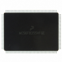
MC56F8355VFGE Freescale Semiconductor, MC56F8355VFGE Datasheet - Page 114

MC56F8355VFGE
Manufacturer Part Number
MC56F8355VFGE
Description
IC DSP 16BIT 60MHZ 128-LQFP
Manufacturer
Freescale Semiconductor
Series
56F8xxxr
Datasheet
1.MC56F8355VFGE.pdf
(172 pages)
Specifications of MC56F8355VFGE
Core Processor
56800
Core Size
16-Bit
Speed
60MHz
Connectivity
CAN, EBI/EMI, SCI, SPI
Peripherals
POR, PWM, Temp Sensor, WDT
Number Of I /o
49
Program Memory Size
264KB (132K x 16)
Program Memory Type
FLASH
Ram Size
10K x 16
Voltage - Supply (vcc/vdd)
2.25 V ~ 3.6 V
Data Converters
A/D 16x12b
Oscillator Type
External
Operating Temperature
-40°C ~ 105°C
Package / Case
128-LQFP
Data Bus Width
16 bit
Processor Series
MC56F83xx
Core
56800E
Numeric And Arithmetic Format
Fixed-Point
Device Million Instructions Per Second
60 MIPs
Maximum Clock Frequency
60 MHz
Number Of Programmable I/os
49
Data Ram Size
20 KB
Maximum Operating Temperature
+ 105 C
Mounting Style
SMD/SMT
Interface Type
SCI, SPI, CAN
Minimum Operating Temperature
- 40 C
For Use With
MC56F8367EVME - EVAL BOARD FOR MC56F83X
Lead Free Status / RoHS Status
Lead free / RoHS Compliant
Eeprom Size
-
Lead Free Status / Rohs Status
Lead free / RoHS Compliant
Available stocks
Company
Part Number
Manufacturer
Quantity
Price
Company:
Part Number:
MC56F8355VFGE
Manufacturer:
Freescale
Quantity:
562
Company:
Part Number:
MC56F8355VFGE
Manufacturer:
Freescale Semiconductor
Quantity:
10 000
Part Number:
MC56F8355VFGE
Manufacturer:
FREESCALE
Quantity:
20 000
6.5.8
The GPIO Peripheral Select register can be used to multiplex out any one of the three alternate peripherals
for GPIOC. The default peripheral is Quad Decoder 1 and Quad Decoder 1, (NOT available in the
56F8155 device); these peripherals work together.
The four I/O pins associated with GPIOC can function as GPIO, Quad Decoder 1/Quad Decoder 1, or as
SPI 1 signals. GPIO is not the default and is enabled/disabled via the GPIOC_PER, as shown in
Figure 6-10
choice between decoder/timer and SPI inputs/outputs is made in the SIM_GPS register and in conjunction
with the Quad Timer Status and Control Registers (SCR). The default state is for the peripheral function
of GPIOC[3:0] to be programmed as decoder functions. This can be changed by altering the appropriate
controls in the indicated registers.
114
GPIO Input
GPIO Output
Quad Timer Input /
Quad Decoder Input
Quad Timer Output /
Quad Decoder Input
Pin Function
GPIO Peripheral Select Register (SIM_GPS)
and
Figure 6-10 Overall Control of Pads Using SIM_GPS Control
Table
2
3
Table 6-2 Control of Pads Using SIM_GPS Control
Quad Timer Controlled
6-2. When GPIOC[3:0] are programmed to operate as peripheral I/O, then the
0
0
1
1
SPI Controlled
—
—
0
1
Control Registers
SIM_ GPS Register
56F8355 Technical Data, Rev. 17
GPIO Controlled
—
—
0
0
0
1
GPIOC_PER Register
—
—
0
1
0
1
See the “Switch Matrix for Inputs to the Timer”
table in the 56F8300 Peripheral User Manual
for the definition of timer inputs based on the
Quad Decoder mode configuration.
I/O Pad Control
Comments
1
Freescale Semiconductor
Preliminary


