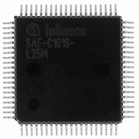
SAF-C161S-L25M AA Infineon Technologies, SAF-C161S-L25M AA Datasheet - Page 17

SAF-C161S-L25M AA
Manufacturer Part Number
SAF-C161S-L25M AA
Description
IC MCU 16BIT ROM/LESS MQFP-80-7
Manufacturer
Infineon Technologies
Series
C16xxr
Datasheet
1.SAF-C161S-L25M_AA.pdf
(75 pages)
Specifications of SAF-C161S-L25M AA
Core Processor
C166
Core Size
16-Bit
Speed
25MHz
Connectivity
EBI/EMI, SPI, UART/USART
Peripherals
POR, PWM, WDT
Number Of I /o
63
Program Memory Type
ROMless
Ram Size
2K x 8
Voltage - Supply (vcc/vdd)
4.5 V ~ 5.5 V
Oscillator Type
External
Operating Temperature
-40°C ~ 85°C
Package / Case
80-SQFP
Data Bus Width
16 bit
Data Ram Size
2 KB
Interface Type
ASC, SSC
Maximum Clock Frequency
25 MHz
Number Of Programmable I/os
63
Number Of Timers
5
Maximum Operating Temperature
+ 85 C
Mounting Style
SMD/SMT
Minimum Operating Temperature
- 40 C
Packages
PG-MQFP-80
Max Clock Frequency
25.0 MHz
Sram (incl. Cache)
2.0 KByte
Program Memory
0.0 KByte
Lead Free Status / RoHS Status
Lead free / RoHS Compliant
Eeprom Size
-
Program Memory Size
-
Data Converters
-
Lead Free Status / Rohs Status
Details
Other names
F161SL25MAAXT
SAF-C161S-L25MAA
SAF-C161S-L25MAAINTR
SAF-C161S-L25MAATR
SAF-C161S-L25MAATR
SAFC161SL25MAAXT
SP000014947
SAF-C161S-L25MAA
SAF-C161S-L25MAAINTR
SAF-C161S-L25MAATR
SAF-C161S-L25MAATR
SAFC161SL25MAAXT
SP000014947
3.3
The main core of the CPU consists of a 4-stage instruction pipeline, a 16-bit arithmetic
and logic unit (ALU) and dedicated SFRs. Additional hardware has been spent for a
separate multiply and divide unit, a bit-mask generator and a barrel shifter.
Based on these hardware provisions, most of the C161S’s instructions can be executed
in just one machine cycle which requires 100 ns at 20 MHz CPU clock. For example,
shift and rotate instructions are always processed during one machine cycle
independent of the number of bits to be shifted. All multiple-cycle instructions have been
optimized so that they can be executed very fast as well: branches in 2 cycles, a
16
pipeline optimization, the so-called ‘Jump Cache’, allows reducing the execution time of
repeatedly performed jumps in a loop from 2 cycles to 1 cycle.
Figure 4
The CPU has a register context consisting of up to 16 wordwide GPRs at its disposal.
These 16 GPRs are physically allocated within the on-chip RAM area. A Context Pointer
(CP) register determines the base address of the active register bank to be accessed by
the CPU at any time. The number of register banks is only restricted by the available
internal RAM space. For easy parameter passing, a register bank may overlap others.
Data Sheet
16 bit multiplication in 5 cycles and a 32-/16-bit division in 10 cycles. Another
ROM
Central Processing Unit (CPU)
CPU Block Diagram
32
Data Page Ptr.
Exec. Unit
Instr. Reg.
SYSCON
Instr. Ptr.
BUSCON 1
BUSCON 0
BUSCON 2
BUSCON 3
BUSCON 4
STKUN
STKOV
PSW
SP
Pipeline
4-Stage
Barrel - Shifter
Bit-Mask Gen
Code Seg. Ptr.
Mul/Div-HW
Context Ptr.
ADDRSEL 1
ADDRSEL 3
ADDRSEL 4
ADDRSEL 2
ALU
MDH
MDL
CPU
13
(16-bit)
Registers
Purpose
General
R15
R0
Functional Description
16
16
V1.0, 2003-11
Internal
RAM
R15
R0
C161S
MCB02147


