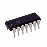
PIC16F526-I/P Microchip Technology, PIC16F526-I/P Datasheet - Page 25

PIC16F526-I/P
Manufacturer Part Number
PIC16F526-I/P
Description
IC PIC MCU FLASH 1KX12 14DIP
Manufacturer
Microchip Technology
Series
PIC® 16Fr
Datasheets
1.PIC16F526-ISL.pdf
(122 pages)
2.PIC16F526-ISL.pdf
(22 pages)
3.PIC16F526-IP.pdf
(104 pages)
Specifications of PIC16F526-I/P
Program Memory Type
FLASH
Program Memory Size
1.5KB (1K x 12)
Package / Case
14-DIP (0.300", 7.62mm)
Core Processor
PIC
Core Size
8-Bit
Speed
20MHz
Peripherals
POR, WDT
Number Of I /o
11
Ram Size
67 x 8
Voltage - Supply (vcc/vdd)
2 V ~ 5.5 V
Data Converters
A/D 3x8b
Oscillator Type
Internal
Operating Temperature
-40°C ~ 85°C
Processor Series
PIC16F
Core
PIC
Data Bus Width
8 bit
Data Ram Size
67 B
Maximum Clock Frequency
20 MHz
Number Of Programmable I/os
12
Number Of Timers
1
Maximum Operating Temperature
+ 85 C
Mounting Style
Through Hole
3rd Party Development Tools
52715-96, 52716-328, 52717-734
Development Tools By Supplier
PG164130, DV164035, DV244005, DV164005, PG164120, ICE2000
Minimum Operating Temperature
- 40 C
On-chip Adc
8 bit, 3 Channel
Lead Free Status / RoHS Status
Lead free / RoHS Compliant
For Use With
AC162096 - HEADER MPLAB ICD2 PIC16F526 8/14
Eeprom Size
-
Connectivity
-
Lead Free Status / Rohs Status
Lead free / RoHS Compliant
5.1
To read a memory location, the user must write the
address to be read into the EEADR register and then
set the RD bit in the EECON register. The data will be
available in the next instruction cycle.
EXAMPLE 5-1:
5.2
In order to write new data to the Flash data memory,
the program memory row that is being addressed by
EEADR<5:0> must be erased.
To prevent a spurious row erasure, a specific
sequence must be executed to initiate the erase to the
program memory. The sequence is as follows:
If the WREN bit is not set in the instruction cycle after
the FREE bit is set, the FREE bit will be cleared in
hardware.
If the WR bit is not set in the instruction cycle after the
WREN bit is set, the WREN bit will be cleared in
hardware.
Both of these sequences is to prevent an accidental
erase of the Flash data memory.
© 2007 Microchip Technology Inc.
INSTRUCTION
Note: Only a BSF command will work to enable the
- Set the FREE bit (enable Flash data memory
- Set the WREN bit (enable writes to the Flash
- set the WR bit (initiates the row erase of the
BSF
MOVLW
BSF
MOVF
row erase)
Data memory array)
Flash data memory array)
Reading Data Memory
Erasing a Data Memory Row
Flash data memory read documented in
Example 5-1. No other sequence of com-
mands will work, no exceptions.
FSR,5
EE_ADR_READ ;LOAD ADDRESS TO READ
EECON,RD
EEDATA,W
FLASH DATA MEMORY
READ
;SWITCH TO BANK 1
;INITITATE THE READ
;IS DECODED
;GET NEW DATA
Preliminary
EXAMPLE 5-2:
5.3
To write a memory location, the user must write the
address to be written to into the EEADR register. He
must then load the data to be written into the EEDATA
register. Once the data and address have been
loaded, a specific sequence must be executed to
initiate the write to the program memory. The
sequence is as follows:
• Set the WREN bit (enable writes to the Flash data
• Set the WR bit (initiates the write to the Flash data
If the WR bit is not set in the instruction cycle after the
WREN bit is set, the WREN bit will be cleared in hard-
ware.
This sequence is to prevent an accidental write to the
Flash memory.
BSF
MOVLW EE_ADR_ERASE ;LOAD ADDRESS TO ERASE
MOVWF EEADR
BSF
BSF
BSF
xxx
Note: The FREE bit may be set by any command
memory array)
memory array)
Writing a Data Memory Word
FSR,5
EECON,FREE
EECON,WREN
EECON,WR
normally used by the core. However, the
WREN and WR bits can only be set using a
series of BSF commands, as documented in
Example 5-2.
commands will work, no exceptions.
ERASE DATA MEMORY
ROW
;SWITCH TO BANK 1
;LOAD ADDRESS TO SFR
;SELECT ERASE
;ENABL FLASH PROG’ING
;INITITATE ERASE
;NEXT INSTRUCTION
No
PIC16F526
other
DS41326A-page 23
sequence
of


