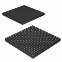
AT91SAM9M10-CU Atmel, AT91SAM9M10-CU Datasheet - Page 17

AT91SAM9M10-CU
Manufacturer Part Number
AT91SAM9M10-CU
Description
IC MCU 16/32BIT ARM9 324TFBGA
Manufacturer
Atmel
Series
AT91SAMr
Specifications of AT91SAM9M10-CU
Core Processor
ARM9
Core Size
16/32-Bit
Speed
400MHz
Connectivity
EBI/EMI, Ethernet, I²C, SPI, SSC, UART/USART, USB
Peripherals
AC'97, DMA, LCD, POR, PWM, WDT
Number Of I /o
160
Program Memory Size
64KB (64K x 8)
Program Memory Type
ROM
Ram Size
128K x 8
Voltage - Supply (vcc/vdd)
0.9 V ~ 1.1 V
Data Converters
A/D 8x10b
Oscillator Type
Internal
Operating Temperature
-40°C ~ 85°C
Package / Case
324-TFBGA
Processor Series
AT91SAMx
Core
ARM926EJ-S
Data Bus Width
32 bit
Data Ram Size
32 KB
Interface Type
2-Wire, SPI, USART
Maximum Clock Frequency
133 MHz
Number Of Programmable I/os
5
Number Of Timers
2 x 16 bit
Operating Supply Voltage
1.65 V to 3.6 V
Maximum Operating Temperature
+ 85 C
Mounting Style
SMD/SMT
3rd Party Development Tools
JTRACE-ARM-2M, MDK-ARM, RL-ARM, ULINK2
Development Tools By Supplier
AT91SAM-ICE, AT91-ISP, AT91SAM9M10-G45-EK
Controller Family/series
AT91
No. Of I/o's
160
Ram Memory Size
64KB
Cpu Speed
400MHz
No. Of Timers
2
Rohs Compliant
Yes
Cpu Family
AT91
Device Core
ARM926EJ-S
Device Core Size
32b
Frequency (max)
400MHz
Total Internal Ram Size
64KB
# I/os (max)
160
Number Of Timers - General Purpose
7
Operating Supply Voltage (typ)
1.8/2.5/3.3V
Operating Supply Voltage (max)
1.1/1.95/3.6V
Operating Supply Voltage (min)
0.9/1.65/1.8/3V
On-chip Adc
8-chx10-bit
Instruction Set Architecture
RISC
Operating Temp Range
-40C to 85C
Operating Temperature Classification
Industrial
Mounting
Surface Mount
Pin Count
324
Package Type
TFBGA
Lead Free Status / RoHS Status
Lead free / RoHS Compliant
Eeprom Size
-
Lead Free Status / Rohs Status
Lead free / RoHS Compliant
Available stocks
Company
Part Number
Manufacturer
Quantity
Price
Company:
Part Number:
AT91SAM9M10-CU
Manufacturer:
Atmel
Quantity:
996
6.2.2
6.2.3
6355BS–ATARM–21-Jun-10
Matrix Slaves
Masters to Slaves Access
Each Slave has its own arbiter, thus allowing a different arbitration per Slave to be programmed.
Table 6-2.
All the Masters can normally access all the Slaves. However, some paths do not make sense,
such as allowing access from the Ethernet MAC to the internal peripherals. Thus, these paths
are forbidden or simply not wired, and shown as “-” in the following tables.
The four DDR ports are connected differently according to the application device.
The user can disable the Video Decoder in the Video Mode Configuration Register (bit
VDEC_SEL) in the Chip Configuration User Interface.
Slave 0
Slave 1
Slave 2
Slave 3
Slave 4
Slave 5
Slave 6
Slave 7
•
•
When the
respectively connected to DDR Port 0 and DDR Port 1. The other masters share DDR Port 2 and DDR
Port 3.
When the
controller, and DDR Port 1 to the LCD controller. The remaining masters share DDR Port 2 and DDR
Port 3.
Video Decoder is not enabled (VDEC_SEL=0)
Video Decoder is enabled (VDEC_SEL=1),
List of Bus Matrix Slaves
Internal SRAM
Internal ROM
USB OHCI
USB EHCI
UDP High Speed RAM
LCD User Interface
Video Decoder
DDR Port 0
DDR Port 1
DDR Port 2
DDR Port 3
External Bus Interface
Internal Peripherals
DDR Port 0 is dedicated to the video
, the ARM instruction and data are
AT91SAM9M10
17


