MC908JL16CPE Freescale Semiconductor, MC908JL16CPE Datasheet - Page 123
MC908JL16CPE
Manufacturer Part Number
MC908JL16CPE
Description
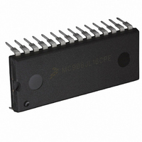
IC MCU 16K FLASH 8MHZ 28-DIP
Manufacturer
Freescale Semiconductor
Series
HC08r
Datasheet
1.MC908JL16CFJER.pdf
(230 pages)
Specifications of MC908JL16CPE
Core Processor
HC08
Core Size
8-Bit
Speed
8MHz
Connectivity
I²C, SCI
Peripherals
LED, LVD, POR, PWM
Number Of I /o
23
Program Memory Size
16KB (16K x 8)
Program Memory Type
FLASH
Ram Size
512 x 8
Voltage - Supply (vcc/vdd)
2.7 V ~ 5.5 V
Data Converters
A/D 12x10b
Oscillator Type
Internal
Operating Temperature
-40°C ~ 85°C
Package / Case
28-DIP (0.600", 15.24mm)
Controller Family/series
HC08
No. Of I/o's
23
Ram Memory Size
512Byte
Cpu Speed
8MHz
No. Of Timers
2
Embedded Interface Type
I2C, SCI
Rohs Compliant
Yes
Processor Series
HC08JL
Core
HC08
Data Bus Width
8 bit
Data Ram Size
512 B
Interface Type
SCI
Maximum Clock Frequency
16 MHz
Number Of Programmable I/os
23
Number Of Timers
4
Operating Supply Voltage
2.7 V to 5.5 V
Maximum Operating Temperature
+ 85 C
Mounting Style
Through Hole
Development Tools By Supplier
FSICEBASE, DEMO908JL16E, M68CBL05CE
Minimum Operating Temperature
- 40 C
On-chip Adc
10 bit, 12 Channel
For Use With
DEMO908JL16E - BOARD DEMO FOR MC908JL16
Lead Free Status / RoHS Status
Lead free / RoHS Compliant
Eeprom Size
-
Lead Free Status / Rohs Status
Details
Available stocks
Company
Part Number
Manufacturer
Quantity
Price
Company:

Part Number:
MC908JL16CPE
Manufacturer:
AMS
Quantity:
183
Part Number:
MC908JL16CPE
Manufacturer:
FREESCALE
Quantity:
20 000


Chapter 9
Analog-to-Digital Converter (ADC)
9.1 Introduction
This section describes the 10-bit successive approximation analog-to-digital converter (ADC10).
The ADC10 on this MCU uses V
as its alternate clock source for the ADC. This MCU does not have a hardware conversion trigger.
9.2 Features
Features of the ADC10 module include:
Figure 9-1
Freescale Semiconductor
$003C
$003D
$003E
$003F
Addr.
•
•
•
•
•
•
•
•
Linear successive approximation algorithm with 10-bit resolution
Output formatted in 10- or 8-bit right-justified format
Single or continuous conversion (automatic power-down in single conversion mode)
Configurable sample time and conversion speed (to save power)
Conversion complete flag and interrupt
Input clock selectable from up to three sources
Operation in wait and stop modes for lower noise operation
Selectable asynchronous hardware conversion trigger
ADC Status and Control Reg-
ADC10 Data Register High
provides a summary of the input/output (I/O) registers.
Register Name
ADC10 Clock Register
ADC10 Data Register
8/10-Bit Mode
(ADCSC)
(ADCLK)
(ADRH)
(ADRL)
ister
Low
Reset:
Reset:
Reset:
Reset:
Read:
Read:
Read:
Read:
Write:
Write:
Write:
Write:
Figure 9-1. ADC I/O Register Summary
DD
ADLPC
COCO
MC68HC908JL16 Data Sheet, Rev. 1.1
and V
Bit 7
AD7
0
0
0
0
0
SS
ADIV1
AIEN
as its supply and reference pins. This MCU uses OSCOUT
AD6
6
0
0
0
0
0
ADCO
ADIV0
AD5
5
0
0
0
0
0
ADICLK
ADCH4
AD4
4
1
0
0
0
0
Reserved
Reserved
MODE1
ADCH3
AD3
3
1
0
0
0
0
MODE0
ADCH2
AD2
2
1
0
0
0
0
ADLSMP
ADCH1
0/AD9
AD1
1
1
0
0
0
ACLKEN
ADCH0
0/AD8
Bit 0
AD0
1
0
0
0
123
Related parts for MC908JL16CPE
Image
Part Number
Description
Manufacturer
Datasheet
Request
R

Part Number:
Description:
Manufacturer:
Freescale Semiconductor, Inc
Datasheet:
Part Number:
Description:
Manufacturer:
Freescale Semiconductor, Inc
Datasheet:
Part Number:
Description:
Manufacturer:
Freescale Semiconductor, Inc
Datasheet:
Part Number:
Description:
Manufacturer:
Freescale Semiconductor, Inc
Datasheet:
Part Number:
Description:
Manufacturer:
Freescale Semiconductor, Inc
Datasheet:
Part Number:
Description:
Manufacturer:
Freescale Semiconductor, Inc
Datasheet:
Part Number:
Description:
Manufacturer:
Freescale Semiconductor, Inc
Datasheet:
Part Number:
Description:
Manufacturer:
Freescale Semiconductor, Inc
Datasheet:
Part Number:
Description:
Manufacturer:
Freescale Semiconductor, Inc
Datasheet:
Part Number:
Description:
Manufacturer:
Freescale Semiconductor, Inc
Datasheet:
Part Number:
Description:
Manufacturer:
Freescale Semiconductor, Inc
Datasheet:
Part Number:
Description:
Manufacturer:
Freescale Semiconductor, Inc
Datasheet:
Part Number:
Description:
Manufacturer:
Freescale Semiconductor, Inc
Datasheet:
Part Number:
Description:
Manufacturer:
Freescale Semiconductor, Inc
Datasheet:
Part Number:
Description:
Manufacturer:
Freescale Semiconductor, Inc
Datasheet: