MC908JL16CPE Freescale Semiconductor, MC908JL16CPE Datasheet - Page 209
MC908JL16CPE
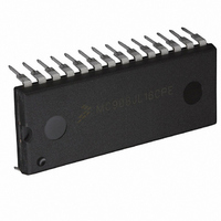
Manufacturer Part Number
MC908JL16CPE
Description
IC MCU 16K FLASH 8MHZ 28-DIP
Manufacturer
Freescale Semiconductor
Series
HC08r
Datasheet
1.MC908JL16CFJER.pdf
(230 pages)
Specifications of MC908JL16CPE
Core Processor
HC08
Core Size
8-Bit
Speed
8MHz
Connectivity
I²C, SCI
Peripherals
LED, LVD, POR, PWM
Number Of I /o
23
Program Memory Size
16KB (16K x 8)
Program Memory Type
FLASH
Ram Size
512 x 8
Voltage - Supply (vcc/vdd)
2.7 V ~ 5.5 V
Data Converters
A/D 12x10b
Oscillator Type
Internal
Operating Temperature
-40°C ~ 85°C
Package / Case
28-DIP (0.600", 15.24mm)
Controller Family/series
HC08
No. Of I/o's
23
Ram Memory Size
512Byte
Cpu Speed
8MHz
No. Of Timers
2
Embedded Interface Type
I2C, SCI
Rohs Compliant
Yes
Processor Series
HC08JL
Core
HC08
Data Bus Width
8 bit
Data Ram Size
512 B
Interface Type
SCI
Maximum Clock Frequency
16 MHz
Number Of Programmable I/os
23
Number Of Timers
4
Operating Supply Voltage
2.7 V to 5.5 V
Maximum Operating Temperature
+ 85 C
Mounting Style
Through Hole
Development Tools By Supplier
FSICEBASE, DEMO908JL16E, M68CBL05CE
Minimum Operating Temperature
- 40 C
On-chip Adc
10 bit, 12 Channel
For Use With
DEMO908JL16E - BOARD DEMO FOR MC908JL16
Lead Free Status / RoHS Status
Lead free / RoHS Compliant
Eeprom Size
-
Lead Free Status / Rohs Status
Details
Available stocks
Company
Part Number
Manufacturer
Quantity
Price
Company:

Part Number:
MC908JL16CPE
Manufacturer:
AMS
Quantity:
183
Part Number:
MC908JL16CPE
Manufacturer:
FREESCALE
Quantity:
20 000


17.9 3-V Control Timing
Freescale Semiconductor
Low-voltage inhibit, trip falling voltage
Low-voltage inhibit, trip rising voltage
Low-voltage inhibit reset/recovery hysteresis
Internal operating frequency
RST input pulse width low
IRQ input pulse width low
TIM2 external clock input
1. V
2. Typical values reflect average measurements at midpoint of voltage range, 25 °C only.
3. Run (operating) I
4. Wait I
5. Stop I
6. Maximum is highest voltage that POR is guaranteed.
7. If minimum V
8. R
1. V
2. Some modules may require a minimum frequency greater than dc for proper operation; see appropriate table for this infor-
3. Minimum pulse width reset is guaranteed to be recognized. It is possible for a smaller pulse width to cause a reset.
Less than 100 pF on all outputs. C
run I
100 pF on all outputs. C
V
noted.
mation.
DD
DD
DD
PU
= 2.7 to 3.3 Vdc, V
DD
= 2.7 to 3.3 Vdc, V
is measured at V
is reached.
DD
DD
. Measured with all modules enabled.
measured using external square wave clock source (f
measured with OSC1 grounded; no port pins sourcing current.
DD
is not reached before the internal POR reset is released, RST must be driven low externally until minimum
DD
Characteristic
measured using external square wave clock source (f
DD
(3)
Characteristic
(3)
SS
SS
L
= 5.0V.
(2)
= 20 pF on OSC2. All ports configured as inputs. OSC2 capacitance linearly affects wait I
= 0 Vdc, T
= 0 Vdc, T
Table 17-7. DC Electrical Characteristics (3V)
(1)
L
A
A
= 20 pF on OSC2. All ports configured as inputs. OSC2 capacitance linearly affects
(1)
= T
= T
Table 17-8. Control Timing (3V)
MC68HC908JL16 Data Sheet, Rev. 1.1
L
L
to T
to T
H
H
; timing shown with respect to 20% V
, unless otherwise noted.
Symbol
V
OP
V
V
TRIPR
TRIPF
HYS
= 4MHz). All inputs 0.2V from rail. No dc loads. Less than
Symbol
f
T2CLK
OP
t
f
t
IRL
OP
IIL
= 4MHz). All inputs 0.2V from rail. No dc loads.
2.475
2.40
Min
—
DD
Min
1.5
1.5
—
—
and 70% V
Typ
2.625
2.55
75
(2)
Max
DD
—
—
4
2
3-V Control Timing
, unless otherwise
2.775
Max
2.70
—
MHz
MHz
Unit
µs
µs
DD
Unit
mV
.
V
V
209
Related parts for MC908JL16CPE
Image
Part Number
Description
Manufacturer
Datasheet
Request
R

Part Number:
Description:
Manufacturer:
Freescale Semiconductor, Inc
Datasheet:
Part Number:
Description:
Manufacturer:
Freescale Semiconductor, Inc
Datasheet:
Part Number:
Description:
Manufacturer:
Freescale Semiconductor, Inc
Datasheet:
Part Number:
Description:
Manufacturer:
Freescale Semiconductor, Inc
Datasheet:
Part Number:
Description:
Manufacturer:
Freescale Semiconductor, Inc
Datasheet:
Part Number:
Description:
Manufacturer:
Freescale Semiconductor, Inc
Datasheet:
Part Number:
Description:
Manufacturer:
Freescale Semiconductor, Inc
Datasheet:
Part Number:
Description:
Manufacturer:
Freescale Semiconductor, Inc
Datasheet:
Part Number:
Description:
Manufacturer:
Freescale Semiconductor, Inc
Datasheet:
Part Number:
Description:
Manufacturer:
Freescale Semiconductor, Inc
Datasheet:
Part Number:
Description:
Manufacturer:
Freescale Semiconductor, Inc
Datasheet:
Part Number:
Description:
Manufacturer:
Freescale Semiconductor, Inc
Datasheet:
Part Number:
Description:
Manufacturer:
Freescale Semiconductor, Inc
Datasheet:
Part Number:
Description:
Manufacturer:
Freescale Semiconductor, Inc
Datasheet:
Part Number:
Description:
Manufacturer:
Freescale Semiconductor, Inc
Datasheet: