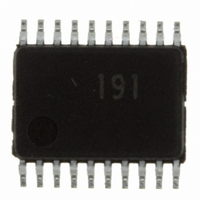
R5F21191SP#U0 Renesas Electronics America, R5F21191SP#U0 Datasheet - Page 16

R5F21191SP#U0
Manufacturer Part Number
R5F21191SP#U0
Description
IC R8C MCU FLASH 8K 20SSOP
Manufacturer
Renesas Electronics America
Series
M16C™ M16C/R8C/Tiny/19r
Datasheets
1.R5F211A2SPU0.pdf
(300 pages)
2.R5F21181DSPU0.pdf
(43 pages)
3.R5F21181DSPU0.pdf
(259 pages)
Specifications of R5F21191SP#U0
Core Processor
R8C
Core Size
16-Bit
Speed
20MHz
Connectivity
SIO, UART/USART
Peripherals
LED, POR, Voltage Detect, WDT
Number Of I /o
13
Program Memory Size
4KB (4K x 8)
Program Memory Type
FLASH
Ram Size
384 x 8
Voltage - Supply (vcc/vdd)
2.7 V ~ 5.5 V
Data Converters
A/D 4x1b
Oscillator Type
Internal
Operating Temperature
-20°C ~ 85°C
Package / Case
20-SSOP
For Use With
R0K521134S000BE - KIT EVAL STARTER FOR R8C/13R0E521174CPE10 - EMULATOR COMPACT R8C/18/19/1
Lead Free Status / RoHS Status
Lead free / RoHS Compliant
Eeprom Size
-
R8C/18 Group, R8C/19 Group
Rev.1.40
REJ03B0124-0140
2.1
2.2
2.3
2.4
2.5
2.6
2.7
2.8
2.8.1
2.8.2
2.8.3
2.8.4
2.8.5
2.8.6
The S flag is set to 1 when an arithmetic operation results in a negative value; otherwise to 0.
The C flag retains a carry, borrow, or shift-out bits that have been generated by the arithmetic and logic
unit.
The Z flag is set to 1 when an arithmetic operation results in 0; otherwise to 0.
Register bank 0 is selected when the B flag is 0. Register bank 1 is selected when this flag is set to 1.
The O flag is set to 1 when the operation results in an overflow; otherwise to 0.
The D flag is for debugging only. Set it to 0.
R0 is a 16-bit register for transfer, arithmetic, and logic operations. The same applies to R1 to R3. R0
can be split into high-order bits (R0H) and low-order bits (R0L) to be used separately as 8-bit data
registers. R1H and R1L are analogous to R0H and R0L. R2 can be combined with R0 and used as a
32-bit data register (R2R0). R3R1 is analogous to R2R0.
A0 is a 16-bit register for address register indirect addressing and address register relative addressing.
It is also used for transfer, arithmetic and logic operations. A1 is analogous to A0. A1 can be combined
with A0 and used as a 32-bit address register (A1A0).
FB is a 16-bit register for FB relative addressing.
INTB is a 20-bit register that indicates the start address of an interrupt vector table.
PC is 20 bits wide, indicates the address of the next instruction to be executed.
The stack pointer (SP), USP, and ISP, are each 16 bits wide. The U flag of FLG is used to switch
between USP and ISP.
SB is a 16-bit register for SB relative addressing.
FLG is an 11-bit register indicating the CPU state.
Data Registers (R0, R1, R2, and R3)
Address Registers (A0 and A1)
Frame Base Register (FB)
Interrupt Table Register (INTB)
Program Counter (PC)
User Stack Pointer (USP) and Interrupt Stack Pointer (ISP)
Static Base Register (SB)
Flag Register (FLG)
Apr 14, 2006
Carry Flag (C)
Debug Flag (D)
Zero Flag (Z)
Sign Flag (S)
Register Bank Select Flag (B)
Overflow Flag (O)
Page 14 of 38
2. Central Processing Unit (CPU)


