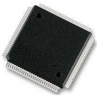
MCF53013CQT240 Freescale Semiconductor, MCF53013CQT240 Datasheet - Page 26

MCF53013CQT240
Manufacturer Part Number
MCF53013CQT240
Description
MCU 32BIT COLDFIRE EMAC 208LQFP
Manufacturer
Freescale Semiconductor
Series
MCF5301xr
Datasheet
1.MCF53010CQT240.pdf
(62 pages)
Specifications of MCF53013CQT240
Core Processor
Coldfire V3
Core Size
32-Bit
Speed
240MHz
Connectivity
EBI/EMI, Ethernet, I²C, MMC, SPI, SSI, UART/USART, USB OTG
Peripherals
DMA, PWM, WDT
Number Of I /o
61
Program Memory Size
16KB (16K x 8)
Program Memory Type
Cache
Ram Size
128K x 8
Voltage - Supply (vcc/vdd)
1.08 V ~ 3.6 V
Oscillator Type
Internal
Operating Temperature
-40°C ~ 85°C
Package / Case
208-LQFP
Processor Series
MCF5301x
Core
ColdFire V3
Data Bus Width
32 bit
Data Ram Size
128 KB
Interface Type
UART, I2C, SPI, SSI, Ethernet
Maximum Clock Frequency
20 MHz to 400 MHz
Number Of Programmable I/os
61
Number Of Timers
8
Operating Supply Voltage
3.6 V
Maximum Operating Temperature
+ 85 C
Mounting Style
SMD/SMT
3rd Party Development Tools
JLINK-CF-BDM26, EWCF
Development Tools By Supplier
M53015EVB, M53017KIT, M53017MOD
Minimum Operating Temperature
- 40 C
Lead Free Status / RoHS Status
Lead free / RoHS Compliant
Eeprom Size
-
Data Converters
-
Preliminary Electrical Characteristics
Chip-select, FB_CS0 can be dedicated to boot ROM access and can be programmed to be byte (8 bits), word (16 bits), or
longword (32 bits) wide. Control signal timing is 1‘compatible with common ROM/flash memories.
5.6.1.1
The following timing numbers indicate when data will be latched or driven onto the external bus, relative to the system clock.
26
1
2
Num
FB1
FB2
FB3
FB4
FB5
FB6
FB7
Timing for chip selects only applies to the FB_CS[5:0] signals. Please see
Characteristics” for SD_CS[3:0] timing.
The FlexBus supports programming an extension of the address hold. Please consult the MCF5301x Reference
Manual for more information.
Frequency of Operation
Clock Period (FB_CLK)
Address, Data, and Control Output Valid (A[23:0], D[31:0],
FB_CS[5:0], R/W, TS, BE/BWE[3:0] and OE)
Address, Data, and Control Output Hold (A[23:0], D[31:0],
FB_CS[5:0], R/W, TS, BE/BWE[3:0], and OE)
Data Input Setup
Data Input Hold
Transfer Acknowledge (TA) Input Setup
Transfer Acknowledge (TA) Input Hold
FlexBus AC Timing Characteristics
The processor drives the data lines during the first clock cycle of the transfer with the full
32-bit address. This may be ignored by standard connected devices using non-multiplexed
address and data buses. However, some applications may find this feature beneficial.
The address and data busses are muxed between the FlexBus and SDRAM controller. At
the end of the read and write bus cycles the address signals are indeterminate.
Characteristic
Table 12. FlexBus AC Timing Specifications
Preliminary—Subject to Change Without Notice
MCF5301x Data Sheet, Rev. 5
NOTE
t
t
Symbol
FBCHDCV
t
t
FBCHDCI
t
t
CVFBCH
DVFBCH
DIFBCH
CIFBCH
t
FBCK
Section 5.7.2, “DDR SDRAM AC Timing
12.5
Min
3.5
—
—
1
0
4
0
Max
7.0
80
—
—
—
—
—
—
Freescale Semiconductor
Unit
Mhz
ns
ns
ns
ns
ns
ns
ns
Notes
f
sys/3
t
1, 2
cyc
1


