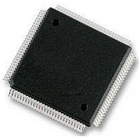
MCF53013CQT240 Freescale Semiconductor, MCF53013CQT240 Datasheet - Page 30

MCF53013CQT240
Manufacturer Part Number
MCF53013CQT240
Description
MCU 32BIT COLDFIRE EMAC 208LQFP
Manufacturer
Freescale Semiconductor
Series
MCF5301xr
Datasheet
1.MCF53010CQT240.pdf
(62 pages)
Specifications of MCF53013CQT240
Core Processor
Coldfire V3
Core Size
32-Bit
Speed
240MHz
Connectivity
EBI/EMI, Ethernet, I²C, MMC, SPI, SSI, UART/USART, USB OTG
Peripherals
DMA, PWM, WDT
Number Of I /o
61
Program Memory Size
16KB (16K x 8)
Program Memory Type
Cache
Ram Size
128K x 8
Voltage - Supply (vcc/vdd)
1.08 V ~ 3.6 V
Oscillator Type
Internal
Operating Temperature
-40°C ~ 85°C
Package / Case
208-LQFP
Processor Series
MCF5301x
Core
ColdFire V3
Data Bus Width
32 bit
Data Ram Size
128 KB
Interface Type
UART, I2C, SPI, SSI, Ethernet
Maximum Clock Frequency
20 MHz to 400 MHz
Number Of Programmable I/os
61
Number Of Timers
8
Operating Supply Voltage
3.6 V
Maximum Operating Temperature
+ 85 C
Mounting Style
SMD/SMT
3rd Party Development Tools
JLINK-CF-BDM26, EWCF
Development Tools By Supplier
M53015EVB, M53017KIT, M53017MOD
Minimum Operating Temperature
- 40 C
Lead Free Status / RoHS Status
Lead free / RoHS Compliant
Eeprom Size
-
Data Converters
-
1
2
3
4
5
6
7
Preliminary Electrical Characteristics
5.7.2
When the SDRAM controller is configured for DDR SDRAM, the following timing numbers must be followed to properly latch
or drive data onto the memory bus. All timing numbers are relative to the four DQS byte lanes. The following timing numbers
are subject to change at anytime, and are only provided to aid in early board design.
30
DD10 Input Data Hold Relative to DQS.
DD11 DQS falling edge from SDCLK rising (output hold time) t
DD12 DQS input read preamble width
DD13 DQS input read postamble width
DD14 DQS output write preamble width
DD15 DQS output write postamble width
Num
DD1
DD2
DD3
DD4
DD5
DD6
DD7
DD8
DD9
The frequency of operation is either 2x or 4x the FB_CLK frequency of operation. FlexBus and SDRAM clock operate at the
same frequency as the internal bus clock.
SD_CLK is one SDRAM clock in (ns).
Pulse width high plus pulse width low cannot exceed min and max clock period.
Command output valid should be 1/2 the memory bus clock (SD_CLK) plus some minor adjustments for process, temperature,
and voltage variations.
This specification relates to the required input setup time of today’s DDR memories. The device’s output setup should be larger
than the input setup of the DDR memories. If it is not larger, then the input setup on the memory will be in violation.
SD_D[31:24] is relative to SD_DQS3, SD_D[23:16] is relative to SD_DQS2, SD_D[15:8] is relative to SD_DQS1, and
SD_D[7:0] is relative SD_DQS0.
The first data beat will be valid before the first rising edge of DQS and after the DQS write preamble. The remaining data beats
will be valid for each subsequent DQS edge.
This specification relates to the required hold time of today’s DDR memories. SD_D[31:24] is relative to SD_DQS3,
SD_D[23:16] is relative to SD_DQS2, SD_D[15:8] is relative to SD_DQS1, and SD_D[7:0] is relative SD_DQS0.
Frequency of Operation
Clock Period
Pulse Width High
Pulse Width Low
Address, SD_CKE, SD_CAS, SD_RAS, SD_WE,
SD_CS[1:0] Output Valid
Address, SD_CKE, SD_CAS, SD_RAS, SD_WE,
SD_CS[1:0] Output Hold
Write Command to first DQS Latching Transition
Data and Data Mask Output Setup (DQ-->DQS)
Relative to DQS (DDR Write Mode)
Data and Data Mask Output Hold (DQS-->DQ)
Relative to DQS (DDR Write Mode)
Input Data Skew Relative to DQS (Input Setup)
DDR SDRAM AC Timing Characteristics
Characteristic
Preliminary—Subject to Change Without Notice
Table 14. DDR Timing Specifications
MCF5301x Data Sheet, Rev. 5
t
t
t
t
t
Symbol
SDCHACV
DQLSDCH
t
t
SDCHACI
CMDVDQ
t
DQWPRE
DQWPST
t
DQRPRE
t
t
DQRPST
DQDMV
t
DDCKH
t
DDCKL
t
DQDMI
t
DDCK
DDSK
DVDQ
DIDQ
0.25 × SD_CLK
+ 0.5ns
12.5
0.45
0.45
0.25
Min
2.0
1.5
1.0
0.5
0.9
0.4
0.4
50
—
—
—
0.5 × SD_CLK
+ 1.0
Max
0.55
0.55
1.25
1.1
0.6
0.6
80
20
—
—
—
—
—
—
1
Freescale Semiconductor
SD_CLK
SD_CLK
SD_CLK
SD_CLK
SD_CLK
SD_CLK
SD_CLK
Unit
Mhz
ns
ns
ns
ns
ns
ns
ns
ns
Notes
1
2
3
3
4
5
6
7
8
9


