M30879FKBGP#U5 Renesas Electronics America, M30879FKBGP#U5 Datasheet - Page 282
M30879FKBGP#U5
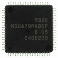
Manufacturer Part Number
M30879FKBGP#U5
Description
IC M32C/87 MCU FLASH 100LQFP
Manufacturer
Renesas Electronics America
Series
M16C™ M32C/80r
Datasheet
1.M3087BFLGPU3.pdf
(629 pages)
Specifications of M30879FKBGP#U5
Core Processor
M32C/80
Core Size
16/32-Bit
Speed
32MHz
Connectivity
EBI/EMI, I²C, IEBus, IrDA, SIO, UART/USART
Peripherals
DMA, POR, PWM, WDT
Number Of I /o
85
Program Memory Size
768KB (768K x 8)
Program Memory Type
FLASH
Ram Size
48K x 8
Voltage - Supply (vcc/vdd)
3 V ~ 5.5 V
Data Converters
A/D 26x10b; D/A 2x8b
Oscillator Type
Internal
Operating Temperature
-20°C ~ 85°C
Package / Case
100-LQFP
For Use With
R0K330879S001BE - KIT DEV RSK M32C/87R0K330879S000BE - KIT DEV RSK M32C/87
Lead Free Status / RoHS Status
Lead free / RoHS Compliant
Eeprom Size
-
Available stocks
Company
Part Number
Manufacturer
Quantity
Price

Part Number:
M30879FKBGP#U5M30879FKBGP#U3
Manufacturer:
Renesas Electronics America
Quantity:
10 000


M32C/87 Group (M32C/87, M32C/87A, M32C/87B)
REJ09B0180-0151 Rev.1.51 Jul 31, 2008
Page 258 of 587
Figure 17.29
17.1.4.3 Clock Phase Setting Function
In master mode
In master mode
(external clock)
(external clock)
(1) When the CKPH = 0 (no clock delay)
(internal clock)
(2) When the CKPH = 1 (clock delay)
(internal clock)
In slave mode
In slave mode
The clock polarity and clock phase are selected from four combinations of the CKPH and CKPOL bits in the
UiSMR3 register (i = 0 to 4). The master must have the same serial clock polarity and phase as the slaves
involved in the communication. Figure 17.29 shows a transmit and receive operation timing.
CLKi I/O (CKPOL = 0)
CLKi I/O (CKPOL = 1)
(DINC = 0)
(DINC = 1)
CLKi I/O (CKPOL = 0)
CLKi I/O (CKPOL = 1)
(DINC = 0)
(DINC = 1)
i=0 to 4
CKPH, DINC: bits in the UiSMR3 register
CKPOL: bit in the UiC0 register
NOTE:
1. P7_0 and P7_1 are N-channel open drain output ports. They must be pulled up externally to output data.
Transmit and Receive Operation Timing in Special Mode 2
SSi input pin
TXDi output
Receive data
input timing
SSi input pin
STXDi output
Receive data
input timing
SSi input pin
TXDi output
Receive data
input timing
SSi input pin
STXDi
output
Receive data
input timing
(1)
(1)
“H”
“L”
“H”
“L”
“H”
“L”
“H”
“L”
“H”
“L”
“H”
“L”
“H”
“L”
“H”
“L”
“H”
“L”
“H”
“L”
“H”
“L”
“H”
“L”
Hi-Z
Hi-Z
undefined
D0
D0
D0
D0
D1
D1
D1
D1
D2
D2
D2
D2
D3
D3
D3
D3
17. Serial Interfaces (UART0 to UART4)
D4
D4
D4
D4
D5
D5
D5
D5
D6
D6
D6
D6
D7
D7
D7
D7
Hi-Z
Hi-Z
Related parts for M30879FKBGP#U5
Image
Part Number
Description
Manufacturer
Datasheet
Request
R

Part Number:
Description:
KIT STARTER FOR M16C/29
Manufacturer:
Renesas Electronics America
Datasheet:

Part Number:
Description:
KIT STARTER FOR R8C/2D
Manufacturer:
Renesas Electronics America
Datasheet:

Part Number:
Description:
R0K33062P STARTER KIT
Manufacturer:
Renesas Electronics America
Datasheet:

Part Number:
Description:
KIT STARTER FOR R8C/23 E8A
Manufacturer:
Renesas Electronics America
Datasheet:

Part Number:
Description:
KIT STARTER FOR R8C/25
Manufacturer:
Renesas Electronics America
Datasheet:

Part Number:
Description:
KIT STARTER H8S2456 SHARPE DSPLY
Manufacturer:
Renesas Electronics America
Datasheet:

Part Number:
Description:
KIT STARTER FOR R8C38C
Manufacturer:
Renesas Electronics America
Datasheet:

Part Number:
Description:
KIT STARTER FOR R8C35C
Manufacturer:
Renesas Electronics America
Datasheet:

Part Number:
Description:
KIT STARTER FOR R8CL3AC+LCD APPS
Manufacturer:
Renesas Electronics America
Datasheet:
Part Number:
Description:
KIT STARTER FOR RX610
Manufacturer:
Renesas Electronics America
Datasheet:

Part Number:
Description:
KIT STARTER FOR R32C/118
Manufacturer:
Renesas Electronics America
Datasheet:

Part Number:
Description:
KIT DEV RSK-R8C/26-29
Manufacturer:
Renesas Electronics America
Datasheet:

Part Number:
Description:
KIT STARTER FOR SH7124
Manufacturer:
Renesas Electronics America
Datasheet:

Part Number:
Description:
KIT STARTER FOR H8SX/1622
Manufacturer:
Renesas Electronics America
Datasheet:

Part Number:
Description:
KIT DEV FOR SH7203
Manufacturer:
Renesas Electronics America
Datasheet: