M30879FKBGP#U5 Renesas Electronics America, M30879FKBGP#U5 Datasheet - Page 616
M30879FKBGP#U5
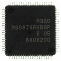
Manufacturer Part Number
M30879FKBGP#U5
Description
IC M32C/87 MCU FLASH 100LQFP
Manufacturer
Renesas Electronics America
Series
M16C™ M32C/80r
Datasheet
1.M3087BFLGPU3.pdf
(629 pages)
Specifications of M30879FKBGP#U5
Core Processor
M32C/80
Core Size
16/32-Bit
Speed
32MHz
Connectivity
EBI/EMI, I²C, IEBus, IrDA, SIO, UART/USART
Peripherals
DMA, POR, PWM, WDT
Number Of I /o
85
Program Memory Size
768KB (768K x 8)
Program Memory Type
FLASH
Ram Size
48K x 8
Voltage - Supply (vcc/vdd)
3 V ~ 5.5 V
Data Converters
A/D 26x10b; D/A 2x8b
Oscillator Type
Internal
Operating Temperature
-20°C ~ 85°C
Package / Case
100-LQFP
For Use With
R0K330879S001BE - KIT DEV RSK M32C/87R0K330879S000BE - KIT DEV RSK M32C/87
Lead Free Status / RoHS Status
Lead free / RoHS Compliant
Eeprom Size
-
Available stocks
Company
Part Number
Manufacturer
Quantity
Price

Part Number:
M30879FKBGP#U5M30879FKBGP#U3
Manufacturer:
Renesas Electronics America
Quantity:
10 000


Rev.
REVISION HISTORY
Date
Page
360
415
432
433
436
439
441
448
449
452
457
469
478
479
484
487
488
490
490
494
495
496
499
500
CAN Module
• NOTE added
Real-Time Port
• Table 24.2 RTP-Associated Register Settings The RTP32 bit function
• Table 24.4 Pin Settings The PS1 register settings modified, note 1
• Table 24.6 Pin Settings P10
Programmable I/O Port
• Figure 25.15 PSC Register Note 1 added
• Figure 25.15 PSC2 Register Note 1 added
• Figure 25.16 PSC3 Register Note 1 added
• Figure 25.19 PUR0 and PUR1 Registers Note 1 modified
• Figure 25.22 IPSA Register Note 1 added
• Table 25.3 Port P6 Peripheral Function Output Control Bit 2 and bit 6
• Table 25.4 Port P7 Peripheral Function Output Control Bit 0 setting in
Flash Memory Version
• 26.2.1 ROM Code Protect Function Description modified
• Figure 26.2 ROMCP Address Bits 5 and 4 functions modified, notes 2 to
• Figure 26.5 FMR1 Register Bits 0, 2 and 3 functions modified
• 26.3.4.5 How to Access Descriptions modified
• Table 26.7 Pin Description P7
Electrical Characteristics
• Table 27.2 Recommended Operating Conditions f(BCLK) standard
• Table 27.3 Electrical Characteristics R
• Table 27.10 Memory Expansion Mode and Microprocessor Mode
• Table 27.22 Memory Expansion Mode and Microprocessor Mode
• Table 27.23 Memory Expansion Mode and Microprocessor Mode
• Figure 27.3 Vcc1=Vcc2=5V Timing Diagram Values in the diagram
• Figure 27.4 Vcc1=Vcc2=5V Timing Diagram Values in the diagram
• Table 27.24 Electrical Characteristics R
• Table 27.25 A/D Conversion Characteristics tCONV standard modified
• Table 27.28 Memory Expansion Mode and Microprocessor Mode
• Table 27.40 Memory Expansion Mode and Microprocessor Mode
• Table 27.41 Memory Expansion Mode and Microprocessor Mode
revised
revised
settings in the PS0 register modified
the PS1 register revised
4 modified, note 5 added
added
standard modified
Formula on note 1 modified
Formula on note 1 modified
Formula on note 1 and 4 modified
modified, note 2 modified
modified, note 1 modified
standard modified
Formula on note 1 modified
Formula on note 1 modified
Formula on note 1 and 4 modified
M32C/87 Group Hardware Manual
C - 5
Description
4
to P10
Summary
6
and P7
7
functions revised
7
PULLUP
functions modified
PULLUP
standard modified, Icc
standard modified, Icc
Related parts for M30879FKBGP#U5
Image
Part Number
Description
Manufacturer
Datasheet
Request
R

Part Number:
Description:
KIT STARTER FOR M16C/29
Manufacturer:
Renesas Electronics America
Datasheet:

Part Number:
Description:
KIT STARTER FOR R8C/2D
Manufacturer:
Renesas Electronics America
Datasheet:

Part Number:
Description:
R0K33062P STARTER KIT
Manufacturer:
Renesas Electronics America
Datasheet:

Part Number:
Description:
KIT STARTER FOR R8C/23 E8A
Manufacturer:
Renesas Electronics America
Datasheet:

Part Number:
Description:
KIT STARTER FOR R8C/25
Manufacturer:
Renesas Electronics America
Datasheet:

Part Number:
Description:
KIT STARTER H8S2456 SHARPE DSPLY
Manufacturer:
Renesas Electronics America
Datasheet:

Part Number:
Description:
KIT STARTER FOR R8C38C
Manufacturer:
Renesas Electronics America
Datasheet:

Part Number:
Description:
KIT STARTER FOR R8C35C
Manufacturer:
Renesas Electronics America
Datasheet:

Part Number:
Description:
KIT STARTER FOR R8CL3AC+LCD APPS
Manufacturer:
Renesas Electronics America
Datasheet:
Part Number:
Description:
KIT STARTER FOR RX610
Manufacturer:
Renesas Electronics America
Datasheet:

Part Number:
Description:
KIT STARTER FOR R32C/118
Manufacturer:
Renesas Electronics America
Datasheet:

Part Number:
Description:
KIT DEV RSK-R8C/26-29
Manufacturer:
Renesas Electronics America
Datasheet:

Part Number:
Description:
KIT STARTER FOR SH7124
Manufacturer:
Renesas Electronics America
Datasheet:

Part Number:
Description:
KIT STARTER FOR H8SX/1622
Manufacturer:
Renesas Electronics America
Datasheet:

Part Number:
Description:
KIT DEV FOR SH7203
Manufacturer:
Renesas Electronics America
Datasheet: