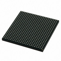
MCIMX512CJM6C Freescale Semiconductor, MCIMX512CJM6C Datasheet - Page 138

MCIMX512CJM6C
Manufacturer Part Number
MCIMX512CJM6C
Description
MULTIMEDIA PROC 529-LFBGA
Manufacturer
Freescale Semiconductor
Series
i.MX51r
Specifications of MCIMX512CJM6C
Core Processor
ARM Cortex-A8
Core Size
32-Bit
Speed
600MHz
Connectivity
1-Wire, EBI/EMI, Ethernet, I²C, IrDA, MMC, SPI, SSI, UART/USART, USB OTG
Peripherals
DMA, I²S, LCD, POR, PWM, WDT
Number Of I /o
128
Program Memory Type
ROMless
Ram Size
128K x 8
Voltage - Supply (vcc/vdd)
0.8 V ~ 1.15 V
Oscillator Type
External
Operating Temperature
-20°C ~ 85°C
Package / Case
529-LFBGA
Operating Temperature (min)
-40C
Operating Temperature Classification
Industrial
Mounting
Surface Mount
Processor Series
i.MX51
Core
ARM Cortex A8
Data Bus Width
32 bit
Program Memory Size
36 KB
Data Ram Size
128 KB
Interface Type
I2C, SPI, SSI, UART, USB
Maximum Clock Frequency
200 MHz
Number Of Timers
5
Operating Supply Voltage
0.8 V to 1.15 V
Maximum Operating Temperature
+ 95 C
Mounting Style
SMD/SMT
3rd Party Development Tools
MDK-ARM, RL-ARM, ULINK2
Development Tools By Supplier
MCIMX51EVKJ
Minimum Operating Temperature
- 40 C
Lead Free Status / RoHS Status
Lead free / RoHS Compliant
Eeprom Size
-
Program Memory Size
-
Data Converters
-
Lead Free Status / Rohs Status
Compliant
- Current page: 138 of 200
- Download datasheet (6Mb)
Electrical Characteristics
4.7.16
Table 106
4.7.16.1 UART Electrical
This section describes the electrical information of the UART module.
138
TXD_MUX
RXD_MUX
DCD
Port
CTS
DTR
DSR
RTS
RI
shows the UART I/O configuration based on which mode is enabled.
UART
•
•
•
•
•
Direction
Output
Output
Output
i.MX51 Applications Processors for Consumer and Industrial Products, Rev. 4
Input
Input
Input
Input
Input
All the timings for the SSI are given for a non-inverted serial clock
polarity (TSCKP/RSCKP = 0) and a non-inverted frame sync
(TFSI/RFSI = 0). If the polarity of the clock and/or the frame sync have
been inverted, all the timing remains valid by inverting the clock signal
STCK/SRCK and/or the frame sync STFS/SRFS shown in the tables
and in the figures.
All timings are on Audiomux Pads when SSI is being used for data
transfer.
“Tx” and “Rx” refer to the Transmit and Receive sections of the SSI.
The terms WL and BL refer to Word Length (WL) and Bit Length (BL).
For internal Frame Sync operation using external clock, the FS timing is
same as that of Tx Data (for example, during AC97 mode of operation).
RTS from DTE to DCE
CTS from DCE to DTE
DTR from DTE to DCE
DSR from DCE to DTE
DCD from DCE to DTE
RING from DCE to DTE
Serial data from DCE to DTE
Serial data from DTE to DCE
Table 106. UART I/O Configuration vs. Mode
DTE Mode
Description
NOTE
Direction
Output
Output
Output
Output
Output
Input
Input
Input
RTS from DTE to DCE
CTS from DCE to DTE
DTR from DTE to DCE
DSR from DCE to DTE
DCD from DCE to DTE
RING from DCE to DTE
Serial data from DCE to DTE
Serial data from DTE to DCE
DCE Mode
Description
Freescale Semiconductor
Related parts for MCIMX512CJM6C
Image
Part Number
Description
Manufacturer
Datasheet
Request
R
Part Number:
Description:
MCIMX-LVDS1
Manufacturer:
Freescale Semiconductor
Datasheet:
Part Number:
Description:
Manufacturer:
Freescale Semiconductor, Inc
Datasheet:
Part Number:
Description:
Manufacturer:
Freescale Semiconductor, Inc
Datasheet:
Part Number:
Description:
Manufacturer:
Freescale Semiconductor, Inc
Datasheet:
Part Number:
Description:
Manufacturer:
Freescale Semiconductor, Inc
Datasheet:
Part Number:
Description:
Manufacturer:
Freescale Semiconductor, Inc
Datasheet:
Part Number:
Description:
Manufacturer:
Freescale Semiconductor, Inc
Datasheet:
Part Number:
Description:
Manufacturer:
Freescale Semiconductor, Inc
Datasheet:
Part Number:
Description:
Manufacturer:
Freescale Semiconductor, Inc
Datasheet:
Part Number:
Description:
Manufacturer:
Freescale Semiconductor, Inc
Datasheet:
Part Number:
Description:
Manufacturer:
Freescale Semiconductor, Inc
Datasheet:
Part Number:
Description:
Manufacturer:
Freescale Semiconductor, Inc
Datasheet:
Part Number:
Description:
Manufacturer:
Freescale Semiconductor, Inc
Datasheet:
Part Number:
Description:
Manufacturer:
Freescale Semiconductor, Inc
Datasheet:
Part Number:
Description:
Manufacturer:
Freescale Semiconductor, Inc
Datasheet:


