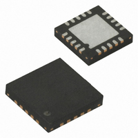
ATTINY2313V-10MUR Atmel, ATTINY2313V-10MUR Datasheet - Page 102

ATTINY2313V-10MUR
Manufacturer Part Number
ATTINY2313V-10MUR
Description
MCU AVR 2KB FLASH 10MHZ 20QFN
Manufacturer
Atmel
Series
AVR® ATtinyr
Specifications of ATTINY2313V-10MUR
Core Processor
AVR
Core Size
8-Bit
Speed
10MHz
Connectivity
SPI, UART/USART
Peripherals
Brown-out Detect/Reset, POR, PWM, WDT
Number Of I /o
18
Program Memory Size
2KB (1K x 16)
Program Memory Type
FLASH
Eeprom Size
128 x 8
Ram Size
128 x 8
Voltage - Supply (vcc/vdd)
1.8 V ~ 5.5 V
Oscillator Type
Internal
Operating Temperature
-40°C ~ 85°C
Package / Case
*
Lead Free Status / RoHS Status
Lead free / RoHS Compliant
Data Converters
-
- Current page: 102 of 226
- Download datasheet (4Mb)
Timer/Counter
Timing Diagrams
102
ATtiny2313
The Timer/Counter is a synchronous design and the timer clock (clk
clock enable signal in the following figures. The figures include information on when interrupt
flags are set, and when the OCR1x Register is updated with the OCR1x buffer value (only for
modes utilizing double buffering).
Figure 49. Timer/Counter Timing Diagram, Setting of OCF1x, no Prescaling
Figure 50
Figure 50. Timer/Counter Timing Diagram, Setting of OCF1x, with Prescaler (f
Figure 51
frequency correct PWM mode the OCR1x Register is updated at BOTTOM. The timing diagrams
will be the same, but TOP should be replaced by BOTTOM, TOP-1 by BOTTOM+1 and so on.
The same renaming applies for modes that set the TOV1 flag at BOTTOM.
TCNTn
OCRnx
OCFnx
OCRnx
(clk
TCNTn
OCFnx
(clk
clk
clk
clk
clk
shows the same timing data, but with the prescaler enabled.
I/O
I/O
shows the count sequence close to TOP in various modes. When using phase and
I/O
Tn
I/O
Tn
/1)
/8)
OCRnx - 1
OCRnx - 1
Figure 49
OCRnx
OCRnx
shows a timing diagram for the setting of OCF1x.
OCRnx Value
OCRnx Value
OCRnx + 1
OCRnx + 1
T1
) is therefore shown as a
OCRnx + 2
OCRnx + 2
clk_I/O
2543L–AVR–08/10
/8)
Related parts for ATTINY2313V-10MUR
Image
Part Number
Description
Manufacturer
Datasheet
Request
R

Part Number:
Description:
IC MCU AVR 2K FLASH 20DIP
Manufacturer:
Atmel
Datasheet:

Part Number:
Description:
IC MCU AVR 2K FLASH 20SOIC
Manufacturer:
Atmel
Datasheet:

Part Number:
Description:
Manufacturer:
Atmel Corporation
Datasheet:

Part Number:
Description:
Manufacturer:
ATMEL Corporation
Datasheet:

Part Number:
Description:
IC MCU AVR 2K FLASH 20MLF
Manufacturer:
Atmel
Datasheet:

Part Number:
Description:
IC MCU AVR 2K FLASH 20DIP
Manufacturer:
Atmel
Datasheet:

Part Number:
Description:
IC MCU AVR 2K FLASH 20SOIC
Manufacturer:
Atmel
Datasheet:

Part Number:
Description:
IC MCU AVR 2K FLASH 20DIP
Manufacturer:
Atmel
Datasheet:

Part Number:
Description:
IC MCU AVR 2K FLASH 20SOIC
Manufacturer:
Atmel
Datasheet:

Part Number:
Description:
IC MCU AVR 2K FLASH 20SOIC
Manufacturer:
Atmel
Datasheet:

Part Number:
Description:
IC MCU AVR 2K FLASH 20WQFN
Manufacturer:
Atmel
Datasheet:

Part Number:
Description:
8-bit AVR Microcontroller with 2K Bytes In-System Programmable Flash
Manufacturer:
ATMEL Corporation
Datasheet:

Part Number:
Description:
Attiny2313 8-bit With 2k Bytes Of In-system Programmable Flash
Manufacturer:
ATMEL Corporation
Datasheet:


