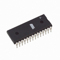
AT89LP828-20PU Atmel, AT89LP828-20PU Datasheet - Page 72

AT89LP828-20PU
Manufacturer Part Number
AT89LP828-20PU
Description
MCU 8051 8K FLASH SPI 28PDIP
Manufacturer
Atmel
Series
89LPr
Datasheet
1.AT89LP428-20AU.pdf
(149 pages)
Specifications of AT89LP828-20PU
Core Processor
8051
Core Size
8-Bit
Speed
20MHz
Connectivity
SPI, UART/USART
Peripherals
Brown-out Detect/Reset, POR, PWM, WDT
Number Of I /o
30
Program Memory Size
8KB (8K x 8)
Program Memory Type
FLASH
Eeprom Size
1K x 8
Ram Size
768 x 8
Voltage - Supply (vcc/vdd)
2.4 V ~ 5.5 V
Oscillator Type
Internal
Operating Temperature
-40°C ~ 85°C
Package / Case
28-DIP (0.300", 7.62mm)
Processor Series
AT89x
Core
8051
Data Bus Width
8 bit
Data Ram Size
768 B
Interface Type
2-Wire, SPI
Maximum Clock Frequency
20 MHz
Number Of Programmable I/os
30
Number Of Timers
3
Maximum Operating Temperature
+ 85 C
Mounting Style
Through Hole
3rd Party Development Tools
PK51, CA51, A51, ULINK2
Development Tools By Supplier
AT89ISP
Minimum Operating Temperature
- 40 C
Lead Free Status / RoHS Status
Lead free / RoHS Compliant
Data Converters
-
Lead Free Status / Rohs Status
Details
Available stocks
Company
Part Number
Manufacturer
Quantity
Price
Company:
Part Number:
AT89LP828-20PU
Manufacturer:
NXP
Quantity:
3 942
13.4.3
Table 13-6.
72
PHS
AT89LP428/828
Multi-Phasic PWM
000
001
010
011
100
2-0
Summary of Multi-Phasic Modes
Figure 13-11. Phase Correct Symmetrical (Center-Aligned) PWM
The PWM channels may be configured to provide multi-phasic alternating outputs by the PHS
bits in T2MOD. The AT89LP428/828 provides 1 out of 2, 1 out of 3, 1 out of 4 and 2 out of 4
phase modes (see
CCD are connected to a one-hot shift register that selectively enables and disables the outputs
(see
as if the compare value was set equal to TOP. The PHSD bit in T2MOD controls the direction of
the shift register. Example waveforms are shown in
multi-phasic PWM, the associated channels must be configured for PWM operation. Non-PWM
channels are not affected by multi-phasic operation. However, their locations in the shift register
are maintained such that some periods in the PWM outputs may not have any pulses as shown
in
The PHS
PHSD are allowed at any time. Note that channels C and D in 1:2 phase mode and channel D in
1:3 phase mode operate normally.
{RCAP2H,RCA2L}
Figure
Figure
{CCxH,CCxL}
Non-Inverted
Mode
2-0
13-14.
Inverted
1:2
1:3
1:4
2:4
Off
13-12). Compare points on disabled channels are blocked from toggling the output
bits may only be modified when the timer is not operational (TR2 = 0). Updates to
CCx
Table
13-6). In Multi-phasic mode, the PWM outputs on CCA, CCB, CCC and
A
→ → → → → → →
B
A
→ → → → →
C
C
CP/RL2 = 0, T2CM
B
A
A
PHSD = 0
Normal Operation (all channels active at all times)
→ → →
→ → →
→ → →
C
D
D
B
B
A
A
A
C
A
B
B
B
B
D
C
C
1-0
= 11B, DCEN = 0
Figure 13-13 on page
D
Behavior
D
→ → → → → → →
C
C
→ → → → →
D
B
B
B
B
PHSD = 1
→ → →
→ → →
→ → →
C
A
A
A
A
73. In order to use
B
C
B
D
D
3654A–MICRO–8/09
Duty Cycle Updated
A
B
A
C
C
A
B
A
2-0


