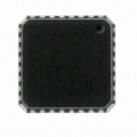
ATTINY26L-8MU Atmel, ATTINY26L-8MU Datasheet - Page 104

ATTINY26L-8MU
Manufacturer Part Number
ATTINY26L-8MU
Description
ID MCU AVR 2K 5V 8MHZ 32-QFN
Manufacturer
Atmel
Series
AVR® ATtinyr
Specifications of ATTINY26L-8MU
Core Processor
AVR
Core Size
8-Bit
Speed
8MHz
Connectivity
USI
Peripherals
Brown-out Detect/Reset, POR, PWM, WDT
Number Of I /o
16
Program Memory Size
2KB (1K x 16)
Program Memory Type
FLASH
Eeprom Size
128 x 8
Ram Size
128 x 8
Voltage - Supply (vcc/vdd)
2.7 V ~ 5.5 V
Data Converters
A/D 11x10b
Oscillator Type
Internal
Operating Temperature
-40°C ~ 85°C
Package / Case
32-VQFN Exposed Pad, 32-HVQFN, 32-SQFN, 32-DHVQFN
Processor Series
ATTINY2x
Core
AVR8
Data Bus Width
8 bit
Data Ram Size
128 B
Interface Type
2-Wire, ISP, SM-Bus, SPI, UART, USI
Maximum Clock Frequency
8 MHz
Number Of Programmable I/os
16
Number Of Timers
2
Operating Supply Voltage
2.7 V to 5.5 V
Maximum Operating Temperature
+ 85 C
Mounting Style
SMD/SMT
3rd Party Development Tools
EWAVR, EWAVR-BL
Development Tools By Supplier
ATAVRDRAGON, ATSTK500, ATSTK600, ATAVRISP2, ATAVRONEKIT
Minimum Operating Temperature
- 40 C
On-chip Adc
10 bit, 11 Channel
Cpu Family
ATtiny
Device Core
AVR
Device Core Size
8b
Frequency (max)
8MHz
Total Internal Ram Size
128Byte
# I/os (max)
16
Number Of Timers - General Purpose
2
Operating Supply Voltage (typ)
3.3/5V
Operating Supply Voltage (max)
5.5V
Operating Supply Voltage (min)
2.7V
Instruction Set Architecture
RISC
Operating Temp Range
-40C to 85C
Operating Temperature Classification
Industrial
Mounting
Surface Mount
Pin Count
32
Package Type
MLF EP
For Use With
ATSTK600 - DEV KIT FOR AVR/AVR32770-1007 - ISP 4PORT ATMEL AVR MCU SPI/JTAGATAVRISP2 - PROGRAMMER AVR IN SYSTEMATSTK505 - ADAPTER KIT FOR 14PIN AVR MCU
Lead Free Status / RoHS Status
Lead free / RoHS Compliant
Other names
ATTINY26L-8MJ
ATTINY26L-8MJ
ATTINY26L-8MJ
Available stocks
Company
Part Number
Manufacturer
Quantity
Price
Part Number:
ATTINY26L-8MU
Manufacturer:
ATMEL/爱特梅尔
Quantity:
20 000
ADC Data Register –
ADCL and ADCH
ADLAR = 0
ADLAR = 1
104
ATtiny26(L)
• Bits 2..0 – ADPS2..0: ADC Prescaler Select Bits
These bits determine the division factor between the CK frequency and the input clock to the
ADC.
Table 47. ADC Prescaler Selections
When an ADC conversion is complete, the result is found in these two registers. The ADLAR bit
in ADMUX affect the way the result is read from the registers. If ADLAR is set, the result is left
adjusted. If ADLAR is cleared (default), the result is right adjusted. If the result is left adjusted
and no more than 8-bit precision is required, it is sufficient to read ADCH. Otherwise, ADCL
must be read first, then ADCH.
• ADC9..0: ADC Conversion Result
These bits represent the result from the conversion. For differential channels, this is the absolute
value after gain adjustment, as indicated in Table 46 on page 102. For single ended channels,
$000 represents analog ground, and $3FF represents the selected reference voltage minus one
LSB.
Bit
$05 ($25)
$04 ($24)
Read/Write
Initial Value
Bit
$05 ($25)
$04 ($24)
Read/Write
Initial Value
ADPS2
0
0
0
0
1
1
1
1
ADC7
ADC9
ADC1
15
15
R
R
R
R
–
7
0
0
7
0
0
ADC6
ADC8
ADC0
14
14
R
R
R
R
–
6
0
0
6
0
0
ADPS1
0
0
1
1
0
0
1
1
ADC5
ADC7
13
13
R
R
R
R
–
5
0
0
–
5
0
0
ADC4
ADC6
12
12
R
R
R
R
–
4
0
0
–
4
0
0
ADPS0
0
1
0
1
0
1
0
1
ADC3
ADC5
11
11
R
R
R
R
–
3
0
0
–
3
0
0
ADC2
ADC4
10
10
R
R
R
R
–
2
0
0
–
2
0
0
ADC9
ADC1
ADC3
Division Factor
R
R
R
R
9
1
0
0
9
–
1
0
0
128
16
32
64
2
2
4
8
ADC8
ADC0
ADC2
R
R
R
R
8
0
0
0
8
–
0
0
0
ADCH
ADCL
ADCH
ADCL
1477K–AVR–08/10


