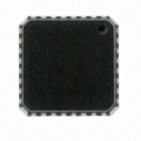
ATTINY26L-8MU Atmel, ATTINY26L-8MU Datasheet - Page 80

ATTINY26L-8MU
Manufacturer Part Number
ATTINY26L-8MU
Description
ID MCU AVR 2K 5V 8MHZ 32-QFN
Manufacturer
Atmel
Series
AVR® ATtinyr
Specifications of ATTINY26L-8MU
Core Processor
AVR
Core Size
8-Bit
Speed
8MHz
Connectivity
USI
Peripherals
Brown-out Detect/Reset, POR, PWM, WDT
Number Of I /o
16
Program Memory Size
2KB (1K x 16)
Program Memory Type
FLASH
Eeprom Size
128 x 8
Ram Size
128 x 8
Voltage - Supply (vcc/vdd)
2.7 V ~ 5.5 V
Data Converters
A/D 11x10b
Oscillator Type
Internal
Operating Temperature
-40°C ~ 85°C
Package / Case
32-VQFN Exposed Pad, 32-HVQFN, 32-SQFN, 32-DHVQFN
Processor Series
ATTINY2x
Core
AVR8
Data Bus Width
8 bit
Data Ram Size
128 B
Interface Type
2-Wire, ISP, SM-Bus, SPI, UART, USI
Maximum Clock Frequency
8 MHz
Number Of Programmable I/os
16
Number Of Timers
2
Operating Supply Voltage
2.7 V to 5.5 V
Maximum Operating Temperature
+ 85 C
Mounting Style
SMD/SMT
3rd Party Development Tools
EWAVR, EWAVR-BL
Development Tools By Supplier
ATAVRDRAGON, ATSTK500, ATSTK600, ATAVRISP2, ATAVRONEKIT
Minimum Operating Temperature
- 40 C
On-chip Adc
10 bit, 11 Channel
Cpu Family
ATtiny
Device Core
AVR
Device Core Size
8b
Frequency (max)
8MHz
Total Internal Ram Size
128Byte
# I/os (max)
16
Number Of Timers - General Purpose
2
Operating Supply Voltage (typ)
3.3/5V
Operating Supply Voltage (max)
5.5V
Operating Supply Voltage (min)
2.7V
Instruction Set Architecture
RISC
Operating Temp Range
-40C to 85C
Operating Temperature Classification
Industrial
Mounting
Surface Mount
Pin Count
32
Package Type
MLF EP
For Use With
ATSTK600 - DEV KIT FOR AVR/AVR32770-1007 - ISP 4PORT ATMEL AVR MCU SPI/JTAGATAVRISP2 - PROGRAMMER AVR IN SYSTEMATSTK505 - ADAPTER KIT FOR 14PIN AVR MCU
Lead Free Status / RoHS Status
Lead free / RoHS Compliant
Other names
ATTINY26L-8MJ
ATTINY26L-8MJ
ATTINY26L-8MJ
Available stocks
Company
Part Number
Manufacturer
Quantity
Price
Part Number:
ATTINY26L-8MU
Manufacturer:
ATMEL/爱特梅尔
Quantity:
20 000
Universal Serial
Interface – USI
Overview
80
ATtiny26(L)
The Universal Serial Interface, or USI, provides the basic hardware resources needed for serial
communication. Combined with a minimum of control software, the USI allows significantly
higher transfer rates and uses less code space than solutions based on software only. Interrupts
are included to minimize the processor load. The main features of the USI are:
•
•
•
•
•
•
A simplified block diagram of the USI is shown on Figure 44.
Figure 44. Universal Serial Interface, Block Diagram
The 8-bit Shift Register is directly accessible via the data bus and contains the incoming and
outgoing data. The register has no buffering so the data must be read as quickly as possible to
ensure that no data is lost. The most significant bit is connected to one of two output pins
depending of the wire mode configuration. A transparent latch is inserted between the serial reg-
ister output and output pin, which delays the change of data output to the opposite clock edge of
the data input sampling. The serial input is always sampled from the Data Input (DI) pin indepen-
dent of the configuration.
The 4-bit counter can be both read and written via the data bus, and can generate an overflow
interrupt. Both the serial register and the counter are clocked simultaneously by the same clock
source. This allows the counter to count the number of bits received or transmitted and generate
an interrupt when the transfer is complete. Note that when an external clock source is selected
the counter counts both clock edges. In this case the counter counts the number of edges, and
not the number of bits. The clock can be selected from three different sources: the SCK pin,
Timer 0 overflow, or from software.
The Two-wire clock control unit can generate an interrupt when a start condition is detected on
the Two-wire bus. It can also generate wait states by holding the clock pin low after a start con-
dition is detected, or after the counter overflows.
Two-wire Synchronous Data Transfer (Master or Slave, f
Three-wire Synchronous Data Transfer (Master, f
Data Received Interrupt
Wakeup from Idle Mode
In Two-wire Mode: Wake-up from All Sleep Modes, Including Power-down Mode
Two-wire Start Condition Detector with Interrupt Capability
USIDR
USISR
USICR
2
4-bit Counter
3
2
1
0
3
2
1
0
D Q
LE
[1]
SCKmax
TIM0 OVF
0
1
= f
SCLmax
CK
/2, Slave f
Two-wire Clock
Control Unit
= f
CK
/16)
CLOCK
HOLD
SCKmax
PB1
PB0
= f
PB2
CK
DO
(Output only)
DI/SDA
(Input/Open Drain)
/4)
SCK/SCL
(Input/Open Drain)
1477K–AVR–08/10


