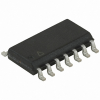
ATTINY44-15SSZ Atmel, ATTINY44-15SSZ Datasheet - Page 53

ATTINY44-15SSZ
Manufacturer Part Number
ATTINY44-15SSZ
Description
IC MCU AVR 4K FLASH 15MHZ 14SOIC
Manufacturer
Atmel
Series
AVR® ATtinyr
Datasheet
1.ATTINY44-15SSZ.pdf
(225 pages)
Specifications of ATTINY44-15SSZ
Core Processor
AVR
Core Size
8-Bit
Speed
16MHz
Connectivity
USI
Peripherals
Brown-out Detect/Reset, POR, PWM, WDT
Number Of I /o
12
Program Memory Size
4KB (2K x 16)
Program Memory Type
FLASH
Eeprom Size
256 x 8
Ram Size
256 x 8
Voltage - Supply (vcc/vdd)
2.7 V ~ 5.5 V
Data Converters
A/D 8x10b
Oscillator Type
Internal
Operating Temperature
-40°C ~ 125°C
Package / Case
14-SOIC (3.9mm Width), 14-SOL
Processor Series
ATTINY4x
Core
AVR8
Data Bus Width
8 bit
Data Ram Size
256 B
Interface Type
SPI, UART
Maximum Clock Frequency
16 MHz
Number Of Programmable I/os
12
Number Of Timers
2
Maximum Operating Temperature
+ 85 C
Mounting Style
SMD/SMT
3rd Party Development Tools
EWAVR, EWAVR-BL
Development Tools By Supplier
ATAVRDRAGON, ATSTK500, ATSTK600, ATAVRISP2, ATAVRONEKIT
Minimum Operating Temperature
- 40 C
On-chip Adc
10 bit, 8 Channel
Lead Free Status / Rohs Status
Details
Other names
Q3447517
Available stocks
Company
Part Number
Manufacturer
Quantity
Price
Company:
Part Number:
ATTINY44-15SSZ
Manufacturer:
ATMEL
Quantity:
350
- Current page: 53 of 225
- Download datasheet (4Mb)
11.2
11.2.1
11.2.2
7701E–AVR–02/11
Register Description
MCUCR – MCU Control Register
GIMSK – General Interrupt Mask Register
The External Interrupt Control Register A contains control bits for interrupt sense control.
• Bits 1, 0 – ISC01, ISC00: Interrupt Sense Control 0 Bit 1 and Bit 0
The External Interrupt 0 is activated by the external pin INT0 if the SREG I-flag and the corre-
sponding interrupt mask are set. The level and edges on the external INT0 pin that activate the
interrupt are defined in
detecting edges. If edge or toggle interrupt is selected, pulses that last longer than one clock
period will generate an interrupt. Shorter pulses are not guaranteed to generate an interrupt. If
low level interrupt is selected, the low level must be held until the completion of the currently
executing instruction to generate an interrupt.
Table 11-1.
• Bits 7, 3..0 – Res: Reserved Bits
These bits are reserved bits in the ATtiny24/44/84 and will always read as zero.
• Bit 6 – INT0: External Interrupt Request 0 Enable
When the INT0 bit is set (one) and the I-bit in the Status Register (SREG) is set (one), the
external pin interrupt is enabled. The Interrupt Sense Control0 bits 1/0 (ISC01 and ISC00) in
the External Interrupt Control Register A (EICRA) define whether the external interrupt is acti-
vated on rising and/or falling edge of the INT0 pin or level sensed. Activity on the pin will cause
an interrupt request even if INT0 is configured as an output. The corresponding interrupt of
External Interrupt Request 0 is executed from the INT0 Interrupt Vector.
• Bit 5 – PCIE1: Pin Change Interrupt Enable 1
When the PCIE1 bit is set (one) and the I-bit in the Status Register (SREG) is set (one), pin
change interrupt 1 is enabled. Any change on any enabled PCINT11..8 pin will cause an inter-
rupt. The corresponding interrupt of Pin Change Interrupt Request is executed from the PCI1
Interrupt Vector. PCINT11..8 pins are enabled individually by the PCMSK1 Register.
Bit
0x35 (0x55)
Read/Write
Initial Value
Bit
0x3B (0x5B)
Read/Write
Initial Value
ISC01
0
0
1
1
Interrupt 0 Sense Control
ISC00
BODS
R/W
7
0
7
–
R
0
0
1
0
1
Table 11-1 on page
PUD
R/W
INT0
R/W
Description
The low level of INT0 generates an interrupt request.
Any logical change on INT0 generates an interrupt request.
The falling edge of INT0 generates an interrupt request.
The rising edge of INT0 generates an interrupt request.
6
0
6
0
Atmel ATtiny24/44/84 [Preliminary]
PCIE1
R/W
R/W
SE
5
0
5
0
PCIE0
SM1
R/W
R/w
4
0
4
0
53. The value on the INT0 pin is sampled before
SM0
R/W
3
0
R
3
–
0
BODSE
R/W
2
0
R
2
–
0
ISC01
R/W
1
0
R
1
–
0
ISC00
R/W
0
0
R
0
–
0
MCUCR
GIMSK
53
Related parts for ATTINY44-15SSZ
Image
Part Number
Description
Manufacturer
Datasheet
Request
R

Part Number:
Description:
Manufacturer:
Atmel Corporation
Datasheet:

Part Number:
Description:
Manufacturer:
Atmel Corporation
Datasheet:

Part Number:
Description:
MCU AVR 4K FLASH 15MHZ 20-QFN
Manufacturer:
Atmel
Datasheet:

Part Number:
Description:
IC MCU AVR 4K FLASH 20MHZ 20-QFN
Manufacturer:
Atmel
Datasheet:

Part Number:
Description:
IC MCU AVR 4K FLASH 20MHZ 14SOIC
Manufacturer:
Atmel
Datasheet:

Part Number:
Description:
MCU AVR 4KB FLASH 20MHZ 14SOIC
Manufacturer:
Atmel
Datasheet:

Part Number:
Description:
MCU AVR 4KB FLASH 20MHZ 20QFN
Manufacturer:
Atmel
Datasheet:

Part Number:
Description:
IC MCU AVR 4K FLASH 20MHZ 14-DIP
Manufacturer:
Atmel
Datasheet:

Part Number:
Description:
IC, MCU, 8BIT, 2K FLASH, 20SOIC
Manufacturer:
Atmel
Datasheet:

Part Number:
Description:
IC, MCU, 8BIT, 2K FLASH, 20PDIP
Manufacturer:
Atmel
Datasheet:

Part Number:
Description:
IC, MCU, 8BIT, 8K FLASH, 20PDIP
Manufacturer:
Atmel
Datasheet:

Part Number:
Description:
IC, MCU, 8BIT, 8K FLASH, 20SOIC
Manufacturer:
Atmel
Datasheet:

Part Number:
Description:
DEV KIT FOR AVR/AVR32
Manufacturer:
Atmel
Datasheet:


