ATTINY861-20SU Atmel, ATTINY861-20SU Datasheet - Page 22

ATTINY861-20SU
Manufacturer Part Number
ATTINY861-20SU
Description
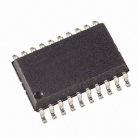
IC MCU AVR 8K FLASH 20MHZ 20SOIC
Manufacturer
Atmel
Series
AVR® ATtinyr
Datasheet
1.ATAVRMC321.pdf
(242 pages)
Specifications of ATTINY861-20SU
Core Processor
AVR
Core Size
8-Bit
Speed
20MHz
Connectivity
USI
Peripherals
Brown-out Detect/Reset, POR, PWM, WDT
Number Of I /o
16
Program Memory Size
8KB (4K x 16)
Program Memory Type
FLASH
Eeprom Size
512 x 8
Ram Size
512 x 8
Voltage - Supply (vcc/vdd)
2.7 V ~ 5.5 V
Data Converters
A/D 11x10b
Oscillator Type
Internal
Operating Temperature
-40°C ~ 85°C
Package / Case
20-SOIC (7.5mm Width)
Cpu Family
ATtiny
Device Core
AVR
Device Core Size
8b
Frequency (max)
20MHz
Interface Type
USI
Total Internal Ram Size
512Byte
# I/os (max)
16
Number Of Timers - General Purpose
2
Operating Supply Voltage (typ)
3.3/5V
Operating Supply Voltage (max)
5.5V
Operating Supply Voltage (min)
2.7V
On-chip Adc
11-chx10-bit
Instruction Set Architecture
RISC
Operating Temp Range
-40C to 85C
Operating Temperature Classification
Industrial
Mounting
Surface Mount
Pin Count
20
Package Type
SOIC
Processor Series
ATTINY8x
Core
AVR8
Data Bus Width
8 bit
Data Ram Size
512 B
Maximum Clock Frequency
20 MHz
Number Of Programmable I/os
16
Number Of Timers
2
Operating Supply Voltage
2.7 V to 5.5 V
Maximum Operating Temperature
+ 85 C
Mounting Style
SMD/SMT
3rd Party Development Tools
EWAVR, EWAVR-BL
Development Tools By Supplier
ATAVRDRAGON, ATSTK500, ATSTK600, ATAVRISP2, ATAVRONEKIT, ATAVRMC320
Minimum Operating Temperature
- 40 C
For Use With
ATSTK600 - DEV KIT FOR AVR/AVR32ATAVRBC100 - REF DESIGN KIT BATTERY CHARGER770-1007 - ISP 4PORT ATMEL AVR MCU SPI/JTAG770-1004 - ISP 4PORT FOR ATMEL AVR MCU SPI
Lead Free Status / RoHS Status
Lead free / RoHS Compliant
Available stocks
Company
Part Number
Manufacturer
Quantity
Price
5.5.5
22
ATtiny261/461/861
GPIOR2 – General Purpose I/O Register 2
old value and program the new value) or to split the Erase and Write operations in two different
operations. The Programming times for the different modes are shown in
Table 5-1.
When EEPE is set, any write to EEPMn will be ignored. During reset, the EEPMn bits will be
reset to 0b00 unless the EEPROM is busy programming.
• Bit 3 – EERIE: EEPROM Ready Interrupt Enable
Writing EERIE to one enables the EEPROM Ready Interrupt if the I-bit in SREG is set. Writing
EERIE to zero disables the interrupt. The EEPROM Ready Interrupt generates a constant inter-
rupt when Non-volatile memory is ready for programming.
• Bit 2 – EEMPE: EEPROM Master Program Enable
The EEMPE bit determines whether writing EEPE to one will have effect or not.
When EEMPE is set, setting EEPE within four clock cycles will program the EEPROM at the
selected address. If EEMPE is zero, setting EEPE will have no effect. When EEMPE has been
written to one by software, hardware clears the bit to zero after four clock cycles.
• Bit 1 – EEPE: EEPROM Program Enable
The EEPROM Program Enable Signal EEPE is the programming enable signal to the EEPROM.
When EEPE is written, the EEPROM will be programmed according to the EEPMn bits setting.
The EEMPE bit must be written to one before a logical one is written to EEPE, otherwise no
EEPROM write takes place. When the write access time has elapsed, the EEPE bit is cleared
by hardware. When EEPE has been set, the CPU is halted for two cycles before the next
instruction is executed.
• Bit 0 – EERE: EEPROM Read Enable
The EEPROM Read Enable Signal – EERE – is the read strobe to the EEPROM. When the cor-
rect address is set up in the EEAR Register, the EERE bit must be written to one to trigger the
EEPROM read. The EEPROM read access takes one instruction, and the requested data is
available immediately. When the EEPROM is read, the CPU is halted for four cycles before the
next instruction is executed. The user should poll the EEPE bit before starting the read opera-
tion. If a write operation is in progress, it is neither possible to read the EEPROM, nor to change
the EEAR Register.
Bit
0x0C (0x2C)
Read/Write
Initial Value
EEPM1
0
0
1
1
EEPM0
EEPROM Mode Bits
0
1
0
1
MSB
R/W
7
0
Programming
R/W
6
0
3.4 ms
1.8 ms
1.8 ms
Time
–
R/W
5
0
Operation
Erase and Write in one operation (Atomic Operation)
Erase Only
Write Only
Reserved for future use
R/W
4
0
R/W
3
0
R/W
2
0
R/W
1
0
Table
LSB
R/W
5-1.
0
0
2588E–AVR–08/10
GPIOR2


