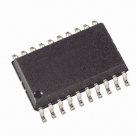
ATTINY861-20SU Atmel, ATTINY861-20SU Datasheet - Page 59

ATTINY861-20SU
Manufacturer Part Number
ATTINY861-20SU
Description
IC MCU AVR 8K FLASH 20MHZ 20SOIC
Manufacturer
Atmel
Series
AVR® ATtinyr
Datasheet
1.ATAVRMC321.pdf
(242 pages)
Specifications of ATTINY861-20SU
Core Processor
AVR
Core Size
8-Bit
Speed
20MHz
Connectivity
USI
Peripherals
Brown-out Detect/Reset, POR, PWM, WDT
Number Of I /o
16
Program Memory Size
8KB (4K x 16)
Program Memory Type
FLASH
Eeprom Size
512 x 8
Ram Size
512 x 8
Voltage - Supply (vcc/vdd)
2.7 V ~ 5.5 V
Data Converters
A/D 11x10b
Oscillator Type
Internal
Operating Temperature
-40°C ~ 85°C
Package / Case
20-SOIC (7.5mm Width)
Cpu Family
ATtiny
Device Core
AVR
Device Core Size
8b
Frequency (max)
20MHz
Interface Type
USI
Total Internal Ram Size
512Byte
# I/os (max)
16
Number Of Timers - General Purpose
2
Operating Supply Voltage (typ)
3.3/5V
Operating Supply Voltage (max)
5.5V
Operating Supply Voltage (min)
2.7V
On-chip Adc
11-chx10-bit
Instruction Set Architecture
RISC
Operating Temp Range
-40C to 85C
Operating Temperature Classification
Industrial
Mounting
Surface Mount
Pin Count
20
Package Type
SOIC
Processor Series
ATTINY8x
Core
AVR8
Data Bus Width
8 bit
Data Ram Size
512 B
Maximum Clock Frequency
20 MHz
Number Of Programmable I/os
16
Number Of Timers
2
Operating Supply Voltage
2.7 V to 5.5 V
Maximum Operating Temperature
+ 85 C
Mounting Style
SMD/SMT
3rd Party Development Tools
EWAVR, EWAVR-BL
Development Tools By Supplier
ATAVRDRAGON, ATSTK500, ATSTK600, ATAVRISP2, ATAVRONEKIT, ATAVRMC320
Minimum Operating Temperature
- 40 C
For Use With
ATSTK600 - DEV KIT FOR AVR/AVR32ATAVRBC100 - REF DESIGN KIT BATTERY CHARGER770-1007 - ISP 4PORT ATMEL AVR MCU SPI/JTAG770-1004 - ISP 4PORT FOR ATMEL AVR MCU SPI
Lead Free Status / RoHS Status
Lead free / RoHS Compliant
Available stocks
Company
Part Number
Manufacturer
Quantity
Price
10.1.5
10.1.6
10.1.7
2588E–AVR–08/10
Digital Input Enable and Sleep Modes
Unconnected Pins
Program Examples
As shown in
schmitt-trigger. The signal denoted SLEEP in the figure, is set by the MCU Sleep Controller in
Power-down mode, Power-save mode, and Standby mode to avoid high power consumption if
some input signals are left floating, or have an analog signal level close to V
SLEEP is overridden for port pins enabled as external interrupt pins. If the external interrupt
request is not enabled, SLEEP is active also for these pins. SLEEP is also overridden by various
other alternate functions as described in
If a logic high level (“one”) is present on an asynchronous external interrupt pin configured as
“Interrupt on Rising Edge, Falling Edge, or Any Logic Change on Pin” while the external interrupt
is not enabled, the corresponding External Interrupt Flag will be set when resuming from the
above mentioned Sleep mode, as the clamping in these sleep mode produces the requested
logic change.
If some pins are unused, it is recommended to ensure that these pins have a defined level. Even
though most of the digital inputs are disabled in the deep sleep modes as described above, float-
ing inputs should be avoided to reduce current consumption in all other modes where the digital
inputs are enabled (Reset, Active mode and Idle mode).
The simplest method to ensure a defined level of an unused pin, is to enable the internal pull-up.
In this case, the pull-up will be disabled during reset. If low power consumption during reset is
important, it is recommended to use an external pull-up or pulldown. Connecting unused pins
directly to V
accidentally configured as an output.
The following code examples show how to set port B pins 0 and 1 high, 2 and 3 low, and define
the port pins from 4 to 5 as input with a pull-up assigned to port pin 4. The resulting pin values
are read back again, but as previously discussed, a nop instruction is included to be able to read
back the value recently assigned to some of the pins.
Note:
Assembly Code Example
...
; Define pull-ups and set outputs high
; Define directions for port pins
ldi
ldi
out
out
; Insert nop for synchronization
nop
; Read port pins
in
...
Two temporary registers are used to minimize the time from pull-ups are set on pins 0, 1 and 4,
until the direction bits are correctly set, defining bit 2 and 3 as low and redefining bits 0 and 1 as
strong high drivers.
CC
Figure
r16,(1<<PB4)|(1<<PB1)|(1<<PB0)
r17,(1<<DDB3)|(1<<DDB2)|(1<<DDB1)|(1<<DDB0)
PORTB,r16
DDRB,r17
r16,PINB
or GND is not recommended, since this may cause excessive currents if the pin is
10-2, the digital input signal can be clamped to ground at the input of the
“Alternate Port Functions” on page
CC
60.
/2.
59


