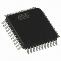
AT89C51RE2-RLTUM Atmel, AT89C51RE2-RLTUM Datasheet - Page 153

AT89C51RE2-RLTUM
Manufacturer Part Number
AT89C51RE2-RLTUM
Description
MCU 8051 128K FLASH 44-VQFP
Manufacturer
Atmel
Series
89Cr
Datasheet
1.AT89C51RE2-SLSUM.pdf
(187 pages)
Specifications of AT89C51RE2-RLTUM
Core Processor
8051
Core Size
8-Bit
Speed
60MHz
Connectivity
I²C, SPI, UART/USART
Peripherals
POR, PWM, WDT
Number Of I /o
34
Program Memory Size
128KB (128K x 8)
Program Memory Type
FLASH
Ram Size
8K x 8
Voltage - Supply (vcc/vdd)
2.7 V ~ 5.5 V
Oscillator Type
External
Operating Temperature
-40°C ~ 85°C
Package / Case
44-TQFP, 44-VQFP
Processor Series
AT89x
Core
8051
Data Bus Width
8 bit
Data Ram Size
8 KB
Interface Type
UART, SPI
Maximum Clock Frequency
60 MHz
Number Of Programmable I/os
34
Number Of Timers
3
Operating Supply Voltage
2.7 V to 5.5 V
Maximum Operating Temperature
+ 85 C
Mounting Style
SMD/SMT
3rd Party Development Tools
PK51, CA51, A51, ULINK2
Development Tools By Supplier
AT89OCD-01
Minimum Operating Temperature
- 40 C
Height
1.45 mm
Length
10.1 mm
Supply Voltage (max)
5.5 V
Supply Voltage (min)
2.7 V
Width
10.1 mm
For Use With
AT89STK-11 - KIT STARTER FOR AT89C51RX2
Lead Free Status / RoHS Status
Lead free / RoHS Compliant
Eeprom Size
-
Data Converters
-
Lead Free Status / Rohs Status
Details
Available stocks
Company
Part Number
Manufacturer
Quantity
Price
Company:
Part Number:
AT89C51RE2-RLTUM
Manufacturer:
MSC
Quantity:
1 560
Figure 59. Data Transmission Format (CPHA = 0)
Figure 60. Data Transmission Format (CPHA = 1)
Figure 61. CPHA/SS Timing
Queuing transmission
7663E–8051–10/08
MOSI (from Master)
SCK Cycle Number
MISO (from Slave)
MOSI (from Master)
SCK (CPOL = 0)
SCK (CPOL = 1)
MISO (from Slave)
SCK Cycle Number
SPEN (Internal)
SCK (CPOL = 0)
SCK (CPOL = 1)
Capture Point
SPEN (Internal)
SS (to Slave)
Capture Point
SS (to Slave)
As shown in Figure 59, the first SCK edge is the MSB capture strobe. Therefore, the Slave must
begin driving its data before the first SCK edge, and a falling edge on the SS pin is used to start
the transmission. The SS pin must be toggled high and then low between each Byte transmitted
(Figure 61).
Figure 60 shows an SPI transmission in which CPHA is’1’. In this case, the Master begins driv-
ing its MOSI pin on the first SCK edge. Therefore, the Slave uses the first SCK edge as a start
transmission signal. The SS pin can remain low between transmissions (Figure 61). This format
may be preferred in systems having only one Master and only one Slave driving the MISO data
line.
For an SPI configured in master or slave mode, a queued data byte must be transmit-
ted/received immediately after the previous transmission has completed.
MISO/MOSI
(CPHA = 0)
(CPHA = 1)
Master SS
Slave SS
Slave SS
MSB
MSB
MSB
1
MSB
1
2
bit6
bit6
2
bit6
Byte 1
bit6
3
bit5
bit5
3
bit5
bit5
bit4
4
bit4
bit4
4
bit4
Byte 2
bit3
bit3
5
bit3
bit3
5
6
bit2
bit2
6
bit2
bit2
Byte 3
7
bit1
bit1
7
bit1
bit1
LSB
8
LSB
LSB
8
LSB
AT89C51RE2
153


