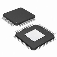
PIC24FJ256DA210-I/PT Microchip Technology, PIC24FJ256DA210-I/PT Datasheet - Page 348

PIC24FJ256DA210-I/PT
Manufacturer Part Number
PIC24FJ256DA210-I/PT
Description
MCU PIC 16BIT FLASH 256K 100TQFP
Manufacturer
Microchip Technology
Series
PIC® 24Fr
Specifications of PIC24FJ256DA210-I/PT
Core Size
16-Bit
Program Memory Size
256KB (85.5K x 24)
Core Processor
PIC
Speed
32MHz
Connectivity
I²C, IrDA, SPI, UART/USART, USB OTG
Peripherals
Brown-out Detect/Reset, GFX, LVD, POR, PWM, WDT
Number Of I /o
84
Program Memory Type
FLASH
Ram Size
96K x 8
Voltage - Supply (vcc/vdd)
2.2 V ~ 3.6 V
Data Converters
A/D 24x10b
Oscillator Type
Internal
Operating Temperature
-40°C ~ 85°C
Package / Case
100-TFQFP
Controller Family/series
PIC24
No. Of I/o's
84
Ram Memory Size
96KB
Cpu Speed
32MHz
No. Of Timers
5
Interface
I2C, SPI, UART, USB
Embedded Interface Type
I2C, SPI, UART, USB
Rohs Compliant
Yes
Processor Series
PIC24FJ
Core
PIC
Data Bus Width
16 bit
Data Ram Size
96 KB
Interface Type
UART, SPI, USB, I2C, RS-485, RS-232
Maximum Clock Frequency
32 MHz
Number Of Programmable I/os
23
Number Of Timers
5
Operating Supply Voltage
3.6 V
Maximum Operating Temperature
+ 85 C
Mounting Style
SMD/SMT
3rd Party Development Tools
52713-733, 52714-737, 53276-922, EWDSPIC
Development Tools By Supplier
PG164130, DV164035, DV244005, DV164005, AC164127-4, AC164127-6, AC164139, DM240001, DM240312, DV164039
Minimum Operating Temperature
- 40 C
Lead Free Status / RoHS Status
Lead free / RoHS Compliant
Eeprom Size
-
Lead Free Status / Rohs Status
Details
Available stocks
Company
Part Number
Manufacturer
Quantity
Price
Company:
Part Number:
PIC24FJ256DA210-I/PT
Manufacturer:
Microchip Technology
Quantity:
10 000
Part Number:
PIC24FJ256DA210-I/PT
Manufacturer:
MICROCHIP/微芯
Quantity:
20 000
- Current page: 348 of 408
- Download datasheet (4Mb)
PIC24FJ256DA210 FAMILY
REGISTER 27-1:
DS39969B-page 348
bit 23
bit 15
bit 7
Legend:
R = Readable bit
-n = Value at POR
bit 23-16
bit 15
bit 14
bit 13
bit 12
bit 11
bit 10
bit 9-8
bit 7
bit 6
bit 5
Note 1:
FWDTEN
reserved
R/PO-1
U-0
r-x
—
Unimplemented in 64-pin devices, maintain at ‘1’ (V
Unimplemented: Read as ‘1’
Reserved: The value is unknown; program as ‘0’
JTAGEN: JTAG Port Enable bit
1 = JTAG port is enabled
0 = JTAG port is disabled
GCP: General Segment Program Memory Code Protection bit
1 = Code protection is disabled
0 = Code protection is enabled for the entire program memory space
GWRP: General Segment Code Flash Write Protection bit
1 = Writes to program memory are allowed
0 = Writes to program memory are not allowed
DEBUG: Background Debugger Enable bit
1 = Device resets into Operational mode
0 = Device resets into Debug mode
Reserved: Always maintain as ‘1’
ICS<1:0>: Emulator Pin Placement Select bits
11 = Emulator functions are shared with PGEC1/PGED1
10 = Emulator functions are shared with PGEC2/PGED2
01 = Emulator functions are shared with PGEC3/PGED3
00 = Reserved; do not use
FWDTEN: Watchdog Timer Enable bit
1 = Watchdog Timer is enabled
0 = Watchdog Timer is disabled
WINDIS: Windowed Watchdog Timer Disable bit
1 = Standard Watchdog Timer is enabled
0 = Windowed Watchdog Timer is enabled; FWDTEN must be ‘1’
ALTVREF: Alternate V
1 = V
0 = V
JTAGEN
WINDIS
R/PO-1
R/PO-1
U-0
—
REF
REF
CW1: FLASH CONFIGURATION WORD 1
is on a default pin (V
is on an alternate pin (V
r = Reserved bit
W = Writable bit
‘1’ = Bit is set
ALTVREF
R/PO-1
R/PO-1
GCP
U-0
—
REF
(1)
Pin Selection bit
REF
R/PO-1
R/PO-1
FWPSA
GWRP
REF
U-0
+ on RA10 and V
—
+ on RB0 and V
(1)
U = Unimplemented bit, read as ‘0’
‘0’ = Bit is cleared
WDTPS3
DEBUG
R/PO-1
R/PO-1
REF
U-0
—
+ on RB0 and V
REF
REF
- on RA9)
- on RB1)
reserved
WDTPS2
R/PO-1
U-0
r-1
—
REF
- on RB1).
2010 Microchip Technology Inc.
x = Bit is unknown
WDTPS1
R/PO-1
R/PO-1
ICS1
U-0
—
WDTPS0
R/PO-1
R/PO-1
ICS0
U-0
—
bit 16
bit 8
bit 0
Related parts for PIC24FJ256DA210-I/PT
Image
Part Number
Description
Manufacturer
Datasheet
Request
R

Part Number:
Description:
Manufacturer:
Microchip Technology Inc.
Datasheet:

Part Number:
Description:
Manufacturer:
Microchip Technology Inc.
Datasheet:

Part Number:
Description:
Manufacturer:
Microchip Technology Inc.
Datasheet:

Part Number:
Description:
Manufacturer:
Microchip Technology Inc.
Datasheet:

Part Number:
Description:
Manufacturer:
Microchip Technology Inc.
Datasheet:

Part Number:
Description:
Manufacturer:
Microchip Technology Inc.
Datasheet:

Part Number:
Description:
Manufacturer:
Microchip Technology Inc.
Datasheet:

Part Number:
Description:
Manufacturer:
Microchip Technology Inc.
Datasheet:


