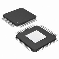
PIC24FJ256DA210-I/PT Microchip Technology, PIC24FJ256DA210-I/PT Datasheet - Page 88

PIC24FJ256DA210-I/PT
Manufacturer Part Number
PIC24FJ256DA210-I/PT
Description
MCU PIC 16BIT FLASH 256K 100TQFP
Manufacturer
Microchip Technology
Series
PIC® 24Fr
Specifications of PIC24FJ256DA210-I/PT
Core Size
16-Bit
Program Memory Size
256KB (85.5K x 24)
Core Processor
PIC
Speed
32MHz
Connectivity
I²C, IrDA, SPI, UART/USART, USB OTG
Peripherals
Brown-out Detect/Reset, GFX, LVD, POR, PWM, WDT
Number Of I /o
84
Program Memory Type
FLASH
Ram Size
96K x 8
Voltage - Supply (vcc/vdd)
2.2 V ~ 3.6 V
Data Converters
A/D 24x10b
Oscillator Type
Internal
Operating Temperature
-40°C ~ 85°C
Package / Case
100-TFQFP
Controller Family/series
PIC24
No. Of I/o's
84
Ram Memory Size
96KB
Cpu Speed
32MHz
No. Of Timers
5
Interface
I2C, SPI, UART, USB
Embedded Interface Type
I2C, SPI, UART, USB
Rohs Compliant
Yes
Processor Series
PIC24FJ
Core
PIC
Data Bus Width
16 bit
Data Ram Size
96 KB
Interface Type
UART, SPI, USB, I2C, RS-485, RS-232
Maximum Clock Frequency
32 MHz
Number Of Programmable I/os
23
Number Of Timers
5
Operating Supply Voltage
3.6 V
Maximum Operating Temperature
+ 85 C
Mounting Style
SMD/SMT
3rd Party Development Tools
52713-733, 52714-737, 53276-922, EWDSPIC
Development Tools By Supplier
PG164130, DV164035, DV244005, DV164005, AC164127-4, AC164127-6, AC164139, DM240001, DM240312, DV164039
Minimum Operating Temperature
- 40 C
Lead Free Status / RoHS Status
Lead free / RoHS Compliant
Eeprom Size
-
Lead Free Status / Rohs Status
Details
Available stocks
Company
Part Number
Manufacturer
Quantity
Price
Company:
Part Number:
PIC24FJ256DA210-I/PT
Manufacturer:
Microchip Technology
Quantity:
10 000
Part Number:
PIC24FJ256DA210-I/PT
Manufacturer:
MICROCHIP/微芯
Quantity:
20 000
- Current page: 88 of 408
- Download datasheet (4Mb)
PIC24FJ256DA210 FAMILY
REGISTER 6-1:
DS39969B-page 88
bit 15
bit 7
Legend:
R = Readable bit
-n = Value at POR
bit 15
bit 14
bit 13-10
bit 9
bit 8
bit 7
bit 6
bit 5
bit 4
bit 3
Note 1:
R/W-0, HS
R/W-0, HS
TRAPR
EXTR
2:
3:
All of the Reset status bits may be set or cleared in software. Setting one of these bits in software does not
cause a device Reset.
If the FWDTEN Configuration bit is ‘1’ (unprogrammed), the WDT is always enabled, regardless of the
SWDTEN bit setting.
Re-enabling the regulator after it enters Standby mode will add a delay, T
Sleep. Applications that do not use the voltage regulator should set this bit to prevent this delay from
occurring.
TRAPR: Trap Reset Flag bit
1 = A Trap Conflict Reset has occurred
0 = A Trap Conflict Reset has not occurred
IOPUWR: Illegal Opcode or Uninitialized W Access Reset Flag bit
1 = An illegal opcode detection, an illegal address mode or uninitialized W register is used as an
0 = An illegal opcode or uninitialized W Reset has not occurred
Unimplemented: Read as ‘0’
CM: Configuration Word Mismatch Reset Flag bit
1 = A Configuration Word Mismatch Reset has occurred
0 = A Configuration Word Mismatch Reset has not occurred
VREGS: Voltage Regulator Standby Enable bit
1 = Program memory and regulator remain active during Sleep/Idle
0 = Program memory power is removed and regulator goes to standby during Seep/Idle
EXTR: External Reset (MCLR) Pin bit
1 = A Master Clear (pin) Reset has occurred
0 = A Master Clear (pin) Reset has not occurred
SWR: Software Reset (Instruction) Flag bit
1 = A RESET instruction has been executed
0 = A RESET instruction has not been executed
SWDTEN: Software Enable/Disable of WDT bit
1 = WDT is enabled
0 = WDT is disabled
WDTO: Watchdog Timer Time-out Flag bit
1 = WDT time-out has occurred
0 = WDT time-out has not occurred
SLEEP: Wake From Sleep Flag bit
1 = Device has been in Sleep mode
0 = Device has not been in Sleep mode
R/W-0, HS
R/W-0, HS
IOPUWR
SWR
Address Pointer and caused a Reset
RCON: RESET CONTROL REGISTER
HS = Hardware Settable bit
W = Writable bit
‘1’ = Bit is set
SWDTEN
R/W-0, HS
U-0
—
(2)
R/W-0, HS
WDTO
U-0
—
U = Unimplemented bit, read as ‘0’
‘0’ = Bit is cleared
R/W-0, HS
(3)
(2)
SLEEP
U-0
—
(1)
R/W-0, HS
IDLE
U-0
—
VREG
2010 Microchip Technology Inc.
x = Bit is unknown
, when waking up from
R/W-0, HS
R/W-1, HS
BOR
CM
R/W-1, HS
VREGS
R/W-0
POR
bit 8
bit 0
(3)
Related parts for PIC24FJ256DA210-I/PT
Image
Part Number
Description
Manufacturer
Datasheet
Request
R

Part Number:
Description:
Manufacturer:
Microchip Technology Inc.
Datasheet:

Part Number:
Description:
Manufacturer:
Microchip Technology Inc.
Datasheet:

Part Number:
Description:
Manufacturer:
Microchip Technology Inc.
Datasheet:

Part Number:
Description:
Manufacturer:
Microchip Technology Inc.
Datasheet:

Part Number:
Description:
Manufacturer:
Microchip Technology Inc.
Datasheet:

Part Number:
Description:
Manufacturer:
Microchip Technology Inc.
Datasheet:

Part Number:
Description:
Manufacturer:
Microchip Technology Inc.
Datasheet:

Part Number:
Description:
Manufacturer:
Microchip Technology Inc.
Datasheet:


