PIC24FJ256DA210-I/PT Microchip Technology, PIC24FJ256DA210-I/PT Datasheet - Page 86
PIC24FJ256DA210-I/PT
Manufacturer Part Number
PIC24FJ256DA210-I/PT
Description
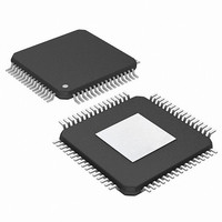
MCU PIC 16BIT FLASH 256K 100TQFP
Manufacturer
Microchip Technology
Series
PIC® 24Fr
Specifications of PIC24FJ256DA210-I/PT
Core Size
16-Bit
Program Memory Size
256KB (85.5K x 24)
Core Processor
PIC
Speed
32MHz
Connectivity
I²C, IrDA, SPI, UART/USART, USB OTG
Peripherals
Brown-out Detect/Reset, GFX, LVD, POR, PWM, WDT
Number Of I /o
84
Program Memory Type
FLASH
Ram Size
96K x 8
Voltage - Supply (vcc/vdd)
2.2 V ~ 3.6 V
Data Converters
A/D 24x10b
Oscillator Type
Internal
Operating Temperature
-40°C ~ 85°C
Package / Case
100-TFQFP
Controller Family/series
PIC24
No. Of I/o's
84
Ram Memory Size
96KB
Cpu Speed
32MHz
No. Of Timers
5
Interface
I2C, SPI, UART, USB
Embedded Interface Type
I2C, SPI, UART, USB
Rohs Compliant
Yes
Processor Series
PIC24FJ
Core
PIC
Data Bus Width
16 bit
Data Ram Size
96 KB
Interface Type
UART, SPI, USB, I2C, RS-485, RS-232
Maximum Clock Frequency
32 MHz
Number Of Programmable I/os
23
Number Of Timers
5
Operating Supply Voltage
3.6 V
Maximum Operating Temperature
+ 85 C
Mounting Style
SMD/SMT
3rd Party Development Tools
52713-733, 52714-737, 53276-922, EWDSPIC
Development Tools By Supplier
PG164130, DV164035, DV244005, DV164005, AC164127-4, AC164127-6, AC164139, DM240001, DM240312, DV164039
Minimum Operating Temperature
- 40 C
Lead Free Status / RoHS Status
Lead free / RoHS Compliant
Eeprom Size
-
Lead Free Status / Rohs Status
Details
Available stocks
Company
Part Number
Manufacturer
Quantity
Price
Company:

Part Number:
PIC24FJ256DA210-I/PT
Manufacturer:
Microchip Technology
Quantity:
10 000
Part Number:
PIC24FJ256DA210-I/PT
Manufacturer:
MICROCHIP/微芯
Quantity:
20 000


PIC24FJ256DA210 FAMILY
5.6.2
If a Flash location has been erased, it can be pro-
grammed using table write instructions to write an
instruction word (24-bit) into the write latch. The
TBLPAG register is loaded with the 8 Most Significant
Bytes (MSB) of the Flash address. The TBLWTL and
TBLWTH instructions write the desired data into the
EXAMPLE 5-5:
EXAMPLE 5-6:
DS39969B-page 86
; Setup a pointer to data Program Memory
; Setup NVMCON for programming one word to data Program Memory
// C example using MPLAB C30
unsigned int offset;
unsigned long progAddr = 0xXXXXXX;
unsigned int progDataL = 0xXXXX;
unsigned char progDataH = 0xXX;
//Set up NVMCON for word programming
NVMCON = 0x4003;
//Set up pointer to the first memory location to be written
TBLPAG = progAddr>>16;
offset = progAddr & 0xFFFF;
//Perform TBLWT instructions to write latches
__builtin_tblwtl(offset, progDataL);
__builtin_tblwth(offset, progDataH);
asm(“DISI #5”);
__builtin_write_NVM();
MOV
MOV
MOV
MOV
MOV
TBLWTL W2, [W0]
TBLWTH W3, [W0++]
MOV
MOV
DISI
MOV.B
MOV
MOV.B
MOV
BSET
NOP
NOP
PROGRAMMING A SINGLE WORD
OF FLASH PROGRAM MEMORY
#tblpage(PROG_ADDR), W0
W0, TBLPAG
#tbloffset(PROG_ADDR), W0
#LOW_WORD_N, W2
#HIGH_BYTE_N, W3
#0x4003, W0
W0, NVMCON
#5
#0x55, W0
W0, NVMKEY
#0xAA, W0
W0, NVMKEY
NVMCON, #WR
PROGRAMMING A SINGLE WORD OF FLASH PROGRAM MEMORY
PROGRAMMING A SINGLE WORD OF FLASH PROGRAM MEMORY
(‘C’ LANGUAGE CODE)
;
;Initialize PM Page Boundary SFR
;Initialize a register with program memory address
;
;
; Write PM low word into program latch
; Write PM high byte into program latch
;
; Set NVMOP bits to 0011
; Disable interrupts while the KEY sequence is written
; Write the key sequence
; Start the write cycle
; Required delays
// Address of word to program
// Data to program lower word
// Write to address low word
// Write to upper byte
// Data to program upper byte
// Initialize NVMCON
// Initialize PM Page Boundary SFR
// Initialize lower word of address
// Block interrupts with priority <7
// for next 5 instructions
// C30 function to perform unlock
// sequence and set WR
write latches and specify the lower 16 bits of the pro-
gram memory address to write to. To configure the
NVMCON register for a word write, set the NVMOP bits
(NVMCON<3:0>) to ‘0011’. The write is performed by
executing the unlock sequence and setting the WR bit
(see Example 5-5). An equivalent procedure in ‘C’
compiler, using the MPLAB C30 compiler and built-in
hardware functions is shown in Example 5-6.
2010 Microchip Technology Inc.
Related parts for PIC24FJ256DA210-I/PT
Image
Part Number
Description
Manufacturer
Datasheet
Request
R

Part Number:
Description:
Manufacturer:
Microchip Technology Inc.
Datasheet:
Part Number:
Description:
Manufacturer:
Microchip Technology Inc.
Datasheet:
Part Number:
Description:
Manufacturer:
Microchip Technology Inc.
Datasheet:
Part Number:
Description:
Manufacturer:
Microchip Technology Inc.
Datasheet:
Part Number:
Description:
Manufacturer:
Microchip Technology Inc.
Datasheet:
Part Number:
Description:
Manufacturer:
Microchip Technology Inc.
Datasheet:
Part Number:
Description:
Manufacturer:
Microchip Technology Inc.
Datasheet:
Part Number:
Description:
Manufacturer:
Microchip Technology Inc.
Datasheet: