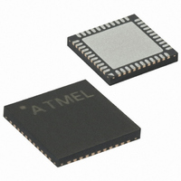
ATMEGA644P-A15MZ Atmel, ATMEGA644P-A15MZ Datasheet - Page 262

ATMEGA644P-A15MZ
Manufacturer Part Number
ATMEGA644P-A15MZ
Description
MCU AVR 64KB FLASH 16MHZ 44QFN
Manufacturer
Atmel
Series
AVR® ATmegar
Specifications of ATMEGA644P-A15MZ
Package / Case
44-VQFN Exposed Pad
Voltage - Supply (vcc/vdd)
2.7 V ~ 5.5 V
Operating Temperature
-40°C ~ 125°C
Speed
16MHz
Number Of I /o
32
Eeprom Size
2K x 8
Core Processor
AVR
Program Memory Type
FLASH
Ram Size
4K x 8
Program Memory Size
64KB (64K x 8)
Data Converters
A/D 8x10b
Oscillator Type
Internal
Peripherals
Brown-out Detect/Reset, POR, PWM, WDT
Connectivity
I²C, SPI, UART/USART
Core Size
8-Bit
Lead Free Status / RoHS Status
Lead free / RoHS Compliant
Available stocks
Company
Part Number
Manufacturer
Quantity
Price
Company:
Part Number:
ATMEGA644P-A15MZ
Manufacturer:
ATMEL
Quantity:
3 500
Part Number:
ATMEGA644P-A15MZ
Manufacturer:
ATMEL/爱特梅尔
Quantity:
20 000
- Current page: 262 of 377
- Download datasheet (7Mb)
21.9.5
262
ATmega164P/324P/644P
DIDR0 – Digital Input Disable Register 0
• Bit 7, 5:3 – Res: Reserved Bits
These bits are reserved for future use in the ATmega164P/324P/644P. For ensuring compability
with future devices, these bits must be written zero when ADCSRB is written.
• Bit 2:0 – ADTS2:0: ADC Auto Trigger Source
If ADATE in ADCSRA is written to one, the value of these bits selects which source will trigger
an ADC conversion. If ADATE is cleared, the ADTS[2:0] settings will have no effect. A conver-
sion will be triggered by the rising edge of the selected Interrupt Flag. Note that switching from a
trigger source that is cleared to a trigger source that is set, will generate a positive edge on the
trigger signal. If ADEN in ADCSRA is set, this will start a conversion. Switching to Free Running
mode (ADTS[2:0]=0) will not cause a trigger event, even if the ADC Interrupt Flag is set
Table 21-6.
• Bit 7..0 – ADC7D..ADC0D: ADC7..0 Digital Input Disable
When this bit is written logic one, the digital input buffer on the corresponding ADC pin is dis-
abled. The corresponding PIN Register bit will always read as zero when this bit is set. When an
analog signal is applied to the ADC7..0 pin and the digital input from this pin is not needed, this
bit should be written logic one to reduce power consumption in the digital input buffer.
Bit
(0x7E)
Read/Write
Initial Value
ADTS2
0
0
0
0
1
1
1
1
ADC7D
ADC Auto Trigger Source Selections
R/W
7
0
ADTS1
0
0
1
1
0
0
1
1
ADC6D
R/W
6
0
ADC5D
ADTS0
R/W
5
0
0
1
0
1
0
1
0
1
ADC4D
R/W
4
0
Trigger Source
Free Running mode
Analog Comparator
External Interrupt Request 0
Timer/Counter0 Compare Match
Timer/Counter0 Overflow
Timer/Counter1 Compare Match B
Timer/Counter1 Overflow
Timer/Counter1 Capture Event
ADC3D
R/W
3
0
ADC2D
R/W
2
0
ADC1D
R/W
1
0
ADC0D
R/W
7674F–AVR–09/09
0
0
.
DIDR0
Related parts for ATMEGA644P-A15MZ
Image
Part Number
Description
Manufacturer
Datasheet
Request
R

Part Number:
Description:
Manufacturer:
Atmel Corporation
Datasheet:

Part Number:
Description:
Manufacturer:
Atmel Corporation
Datasheet:

Part Number:
Description:
IC MCU AVR 64K FLASH 44-TQFP
Manufacturer:
Atmel
Datasheet:

Part Number:
Description:
IC MCU AVR 64K FLASH 44-QFN
Manufacturer:
Atmel
Datasheet:

Part Number:
Description:
MCU AVR 64K FLASH 20MHZ 44-TQFP
Manufacturer:
Atmel
Datasheet:

Part Number:
Description:
IC MCU AVR 64K FLASH 40-DIP
Manufacturer:
Atmel
Datasheet:

Part Number:
Description:
MCU AVR 64K FLASH 20MHZ 44TQFP
Manufacturer:
Atmel
Datasheet:

Part Number:
Description:
MCU AVR 64K FLASH 20MHZ 44QFN
Manufacturer:
Atmel
Datasheet:

Part Number:
Description:
MCU AVR 64K FLASH 20MHZ 44-QFN
Manufacturer:
Atmel
Datasheet:

Part Number:
Description:
MCU AVR 64K FLASH 20MHZ 40-PDIP
Manufacturer:
Atmel
Datasheet:

Part Number:
Description:
MCU AVR 64K FLASH 15MHZ 44-TQFP
Manufacturer:
Atmel
Datasheet:


