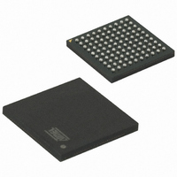
AT91SAM7X512-CU Atmel, AT91SAM7X512-CU Datasheet - Page 509

AT91SAM7X512-CU
Manufacturer Part Number
AT91SAM7X512-CU
Description
MCU ARM 512K HS FLASH 100-TFBGA
Manufacturer
Atmel
Series
AT91SAMr
Datasheet
1.AT91SAM7X512-AU-999.pdf
(687 pages)
Specifications of AT91SAM7X512-CU
Core Processor
ARM7
Core Size
16/32-Bit
Speed
55MHz
Connectivity
CAN, Ethernet, I²C, SPI, SSC, UART/USART, USB
Peripherals
Brown-out Detect/Reset, DMA, POR, PWM, WDT
Number Of I /o
62
Program Memory Size
512KB (512K x 8)
Program Memory Type
FLASH
Ram Size
128K x 8
Voltage - Supply (vcc/vdd)
1.65 V ~ 1.95 V
Data Converters
A/D 8x10b
Oscillator Type
Internal
Operating Temperature
-40°C ~ 85°C
Package / Case
100-TFBGA
Processor Series
AT91SAMx
Core
ARM7TDMI
Data Bus Width
32 bit
Data Ram Size
128 KB
Interface Type
CAN, SPI, SSC, TWI, USART, USB
Maximum Clock Frequency
55 MHz
Number Of Programmable I/os
13
Number Of Timers
3
Operating Supply Voltage
3 V to 3.6 V
Maximum Operating Temperature
+ 85 C
Mounting Style
SMD/SMT
3rd Party Development Tools
JTRACE-ARM-2M, KSK-AT91SAM7X-PL, MDK-ARM, RL-ARM, ULINK2
Development Tools By Supplier
AT91SAM-ICE, AT91-ISP, AT91SAM7X-EK
Minimum Operating Temperature
- 40 C
On-chip Adc
10 bit
Package
100TFBGA
Device Core
ARM7TDMI
Family Name
91S
Maximum Speed
55 MHz
Cpu Family
91S
Device Core Size
32b
Frequency (max)
55MHz
Total Internal Ram Size
128KB
# I/os (max)
62
Number Of Timers - General Purpose
3
Operating Supply Voltage (typ)
1.8/3.3V
Operating Supply Voltage (max)
1.95/3.6V
Operating Supply Voltage (min)
1.65/3V
Instruction Set Architecture
RISC
Operating Temp Range
-40C to 85C
Operating Temperature Classification
Industrial
Mounting
Surface Mount
Pin Count
100
Package Type
TFBGA
For Use With
AT91SAM-ICE - EMULATOR FOR AT91 ARM7/ARM9AT91SAM7X-EK - KIT EVAL FOR AT91SAM7X256/128
Lead Free Status / RoHS Status
Lead free / RoHS Compliant
Eeprom Size
-
Lead Free Status / Rohs Status
Lead free / RoHS Compliant
Available stocks
Company
Part Number
Manufacturer
Quantity
Price
- Current page: 509 of 687
- Download datasheet (11Mb)
6120H–ATARM–17-Feb-09
Figure 36-3. Message Acceptance Procedure
If a mailbox is dedicated to receiving several messages (a family of messages) with different
IDs, the acceptance mask defined in the CAN_MAMx register must mask the variable part of the
ID family. Once a message is received, the application must decode the masked bits in the
CAN_MIDx. To speed up the decoding, masked bits are grouped in the family ID register
(CAN_MFIDx).
For example, if the following message IDs are handled by the same mailbox:
The CAN_MIDx and CAN_MAMx of Mailbox x must be initialized to the corresponding values:
If Mailbox x receives a message with ID6, then CAN_MIDx and CAN_MFIDx are set:
If the application associates a handler for each message ID, it may define an array of pointers to
functions:
When a message is received, the corresponding handler can be invoked using CAN_MFIDx reg-
ister and there is no need to check masked bits:
ID0 101000100100010010000100 0 11 00b
ID1 101000100100010010000100 0 11 01b
ID2 101000100100010010000100 0 11 10b
ID3 101000100100010010000100 0 11 11b
ID4 101000100100010010000100 1 11 00b
ID5 101000100100010010000100 1 11 01b
ID6 101000100100010010000100 1 11 10b
ID7 101000100100010010000100 1 11 11b
CAN_MIDx = 001 101000100100010010000100 x 11 xxb
CAN_MAMx = 001 111111111111111111111111 0 11 00b
CAN_MIDx = 001 101000100100010010000100 1 11 10b
CAN_MFIDx = 00000000000000000000000000000110b
void (*pHandler[8])(void);
unsigned int MFID0_register;
MFID0_register = Get_CAN_MFID0_Register();
// Get_CAN_MFID0_Register() returns the value of the CAN_MFID0 register
pHandler[MFID0_register]();
CAN_MFIDx
CAN_MIDx
AT91SAM7X512/256/128 Preliminary
Message Accepted
&
CAN_MAMx
==
Yes
No
&
Message Received
Message Refused
509
Related parts for AT91SAM7X512-CU
Image
Part Number
Description
Manufacturer
Datasheet
Request
R

Part Number:
Description:
KIT EVAL FOR AT91SAM7X256/128
Manufacturer:
Atmel
Datasheet:

Part Number:
Description:
MCU, MPU & DSP Development Tools KICKSTART KIT ATMEL AT91SAM7X
Manufacturer:
IAR Systems

Part Number:
Description:
DEV KIT FOR AVR/AVR32
Manufacturer:
Atmel
Datasheet:

Part Number:
Description:
INTERVAL AND WIPE/WASH WIPER CONTROL IC WITH DELAY
Manufacturer:
ATMEL Corporation
Datasheet:

Part Number:
Description:
Low-Voltage Voice-Switched IC for Hands-Free Operation
Manufacturer:
ATMEL Corporation
Datasheet:

Part Number:
Description:
MONOLITHIC INTEGRATED FEATUREPHONE CIRCUIT
Manufacturer:
ATMEL Corporation
Datasheet:

Part Number:
Description:
AM-FM Receiver IC U4255BM-M
Manufacturer:
ATMEL Corporation
Datasheet:

Part Number:
Description:
Monolithic Integrated Feature Phone Circuit
Manufacturer:
ATMEL Corporation
Datasheet:

Part Number:
Description:
Multistandard Video-IF and Quasi Parallel Sound Processing
Manufacturer:
ATMEL Corporation
Datasheet:

Part Number:
Description:
High-performance EE PLD
Manufacturer:
ATMEL Corporation
Datasheet:

Part Number:
Description:
8-bit Flash Microcontroller
Manufacturer:
ATMEL Corporation
Datasheet:

Part Number:
Description:
2-Wire Serial EEPROM
Manufacturer:
ATMEL Corporation
Datasheet:


