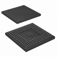
AT91SAM9XE256-CU Atmel, AT91SAM9XE256-CU Datasheet - Page 16

AT91SAM9XE256-CU
Manufacturer Part Number
AT91SAM9XE256-CU
Description
MCU ARM9 256K FLASH 217-BGA
Manufacturer
Atmel
Series
AT91SAMr
Specifications of AT91SAM9XE256-CU
Core Processor
ARM9
Core Size
16/32-Bit
Speed
180MHz
Connectivity
EBI/EMI, Ethernet, I²C, MMC, SPI, SSC, UART/USART, USB
Peripherals
Brown-out Detect/Reset, POR, PWM, WDT
Number Of I /o
96
Program Memory Size
256KB (256K x 8)
Program Memory Type
FLASH
Ram Size
56K x 8
Voltage - Supply (vcc/vdd)
1.65 V ~ 1.95 V
Data Converters
A/D 4x10b
Oscillator Type
Internal
Operating Temperature
-40°C ~ 85°C
Package / Case
217-LFBGA
Processor Series
AT91SAMx
Core
ARM926EJ-S
Data Bus Width
32 bit
Data Ram Size
32 KB
Interface Type
2-Wire, EBI, I2S, SPI, USART
Maximum Clock Frequency
180 MHz
Number Of Programmable I/os
96
Number Of Timers
6
Maximum Operating Temperature
+ 85 C
Mounting Style
SMD/SMT
3rd Party Development Tools
JTRACE-ARM-2M, KSK-AT91SAM9XE-PL, MDK-ARM, RL-ARM, ULINK2
Development Tools By Supplier
AT91SAM-ICE, AT91-ISP, AT91SAM9XE-EK
Minimum Operating Temperature
- 40 C
On-chip Adc
10 bit, 4 Channel
Package
217LFBGA
Device Core
ARM926EJ-S
Family Name
91S
Maximum Speed
180 MHz
Operating Supply Voltage
1.8|2.5|3.3 V
For Use With
AT91SAM9XE-EK - KIT EVAL FOR AT91SAM9XEAT91SAM-ICE - EMULATOR FOR AT91 ARM7/ARM9
Lead Free Status / RoHS Status
Lead free / RoHS Compliant
Eeprom Size
-
Lead Free Status / Rohs Status
Lead free / RoHS Compliant
Available stocks
Company
Part Number
Manufacturer
Quantity
Price
Company:
Part Number:
AT91SAM9XE256-CU
Manufacturer:
ATMEL
Quantity:
215
6.2
6.3
7. Processor and Architecture
7.1
16
I/O Line Drive Levels
Shutdown Logic Pins
ARM926EJ-S Processor
AT91SAM9XE128/256/512 Preliminary
The PIO lines PA0 to PA31 and PB0 to PB31 and PC0 to PC3 are high-drive current capable.
Each of these I/O lines can drive up to 16 mA permanently with a total of 350 mA on all I/O lines.
Refer to the “DC Characteristics” section of the product datasheet.
The SHDN pin is a tri-state output only pin, which is driven by the Shutdown Controller. There is
no internal pull-up. An external pull-up to VDDBU is needed and its value must be higher than
1 MΩ. The resisitor value is calculated according to the regulator enable implementation and the
SHDN level.
The WKUP pin is an input-only. It can accept voltages only between 0V and VDDBU.
• RISC Processor Based on ARM v5TEJ Architecture with Jazelle technology for Java
• Two Instruction Sets
• DSP Instruction Extensions
• 5-Stage Pipeline Architecture:
• 8 Kbytes Data Cache, 16 Kbytes Instruction Cache
• Write Buffer
• Standard ARM v4 and v5 Memory Management Unit (MMU)
• Bus Interface Unit (BIU)
acceleration
– ARM High-performance 32-bit Instruction Set
– Thumb High Code Density 16-bit Instruction Set
– Instruction Fetch (F)
– Instruction Decode (D)
– Execute (E)
– Data Memory (M)
– Register Write (W)
– Virtually-addressed 4-way Associative Cache
– Eight words per line
– Write-through and Write-back Operation
– Pseudo-random or Round-robin Replacement
– Main Write Buffer with 16-word Data Buffer and 4-address Buffer
– DCache Write-back Buffer with 8-word Entries and a Single Address Entry
– Software Control Drain
– Access Permission for Sections
– Access Permission for large pages and small pages can be specified separately for
– 16 embedded domains
each quarter of the page
6254CS–ATARM–08-Jan-10


