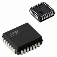
P89LPC936FA,529 NXP Semiconductors, P89LPC936FA,529 Datasheet - Page 8

P89LPC936FA,529
Manufacturer Part Number
P89LPC936FA,529
Description
IC 80C51 MCU FLASH 16K 28-PLCC
Manufacturer
NXP Semiconductors
Series
LPC900r
Datasheet
1.P89LPC936FDH518.pdf
(77 pages)
Specifications of P89LPC936FA,529
Program Memory Type
FLASH
Program Memory Size
16KB (16K x 8)
Package / Case
28-PLCC
Core Processor
8051
Core Size
8-Bit
Speed
18MHz
Connectivity
I²C, SPI, UART/USART
Peripherals
Brown-out Detect/Reset, LED, POR, PWM, WDT
Number Of I /o
26
Eeprom Size
512 x 8
Ram Size
768 x 8
Voltage - Supply (vcc/vdd)
2.4 V ~ 3.6 V
Data Converters
A/D 8x8b; D/A 2x8b
Oscillator Type
Internal
Operating Temperature
-40°C ~ 85°C
Processor Series
P89LPC9x
Core
80C51
Data Bus Width
8 bit
Data Ram Size
768 B
Interface Type
I2C/SPI/UART
Maximum Clock Frequency
18 MHz
Number Of Programmable I/os
26
Number Of Timers
2
Operating Supply Voltage
2.4 V to 3.6 V
Maximum Operating Temperature
+ 85 C
Mounting Style
SMD/SMT
3rd Party Development Tools
PK51, CA51, A51, ULINK2
Minimum Operating Temperature
- 40 C
On-chip Adc
8-ch x 8-bit
Lead Free Status / RoHS Status
Lead free / RoHS Compliant
For Use With
622-1014 - BOARD FOR LPC9XX TSSOP622-1008 - BOARD FOR LPC9103 10-HVSON622-1006 - SOCKET ADAPTER BOARDMCB900K - BOARD PROTOTYPE NXP 89LPC9EPM900K - EMULATOR/PROGRAMMER NXP P89LPC9568-1759 - EMULATOR DEBUGGER/PROGRMMR LPC9X568-1758 - BOARD EVAL FOR LPC93X MCU FAMILY
Lead Free Status / Rohs Status
Lead free / RoHS Compliant
Other names
935278702529
P89LPC936FA-S
P89LPC936FA-S
P89LPC936FA-S
P89LPC936FA-S
Available stocks
Company
Part Number
Manufacturer
Quantity
Price
Company:
Part Number:
P89LPC936FA,529
Manufacturer:
NXP Semiconductors
Quantity:
10 000
NXP Semiconductors
Table 4.
P89LPC933_934_935_936
Product data sheet
Symbol
P1.0 to P1.7
P1.0/TXD
P1.1/RXD
P1.2/T0/SCL 12
P1.3/INT0/
SDA
P1.4/INT1
P1.5/RST
P1.6/OCB
P1.7/OCC/
AD00
Pin description
Pin
TSSOP28,
PLCC28
18
17
11
10
6
5
4
HVQFN28
14
13
8
7
6
2
1
28
…continued
Type
I/O
O
I/O
I
I/O
I/O
I/O
I/O
I
I/O
I
I
I
I
I/O
O
I/O
O
I
I/O, I
All information provided in this document is subject to legal disclaimers.
[1]
Description
Port 1: Port 1 is an 8-bit I/O port with a user-configurable output type,
except for three pins as noted below. During reset Port 1 latches are
configured in the input only mode with the internal pull-up disabled. The
operation of the configurable Port 1 pins as inputs and outputs depends
upon the port configuration selected. Each of the configurable port pins
are programmed independently. Refer to
configurations”
P1.3 are open drain when used as outputs. P1.5 is input only.
All pins have Schmitt trigger inputs.
Port 1 also provides various special functions as described below:
P1.0 — Port 1 bit 0.
TXD — Transmitter output for the serial port.
P1.1 — Port 1 bit 1.
RXD — Receiver input for the serial port.
P1.2 — Port 1 bit 2 (open-drain when used as output).
T0 — Timer/counter 0 external count input or overflow output (open-drain
when used as output).
SCL — I
P1.3 — Port 1 bit 3 (open-drain when used as output).
INT0 — External interrupt 0 input.
SDA — I
P1.4 — Port 1 bit 4.
INT1 — External interrupt 1 input.
P1.5 — Port 1 bit 5 (input only).
RST — External reset input during power-on or if selected via UCFG1.
When functioning as a reset input, a LOW on this pin resets the
microcontroller, causing I/O ports and peripherals to take on their default
states, and the processor begins execution at address 0. Also used during
a power-on sequence to force ISP mode. When using an oscillator
frequency above 12 MHz, the reset input function of P1.5 must be
enabled. An external circuit is required to hold the device in reset at
power-up until VDD has reached its specified level. When system
power is removed VDD will fall below the minimum specified
operating voltage. When using an oscillator frequency above
12 MHz, in some applications, an external brownout detect circuit
may be required to hold the device in reset when VDD falls below the
minimum specified operating voltage.
P1.6 — Port 1 bit 6.
OCB — Output Compare B. (P89LPC935/936)
P1.7 — Port 1 bit 7.
OCC — Output Compare C. (P89LPC935/936)
AD00 — ADC0 channel 0 analog input. (P89LPC935/936)
Rev. 8 — 12 January 2011
8-bit microcontroller with accelerated two-clock 80C51 core
2
2
C serial clock input/output.
C serial data input/output.
and
P89LPC933/934/935/936
Table 11 “Static characteristics”
Section 8.13.1 “Port
for details. P1.2 and
© NXP B.V. 2011. All rights reserved.
8 of 77


