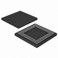
LPC2880FET180,551 NXP Semiconductors, LPC2880FET180,551 Datasheet - Page 7

LPC2880FET180,551
Manufacturer Part Number
LPC2880FET180,551
Description
IC ARM7 MCU RAM 16K 180TFBGA
Manufacturer
NXP Semiconductors
Series
LPC2800r
Datasheet
1.LPC2880FET180551.pdf
(43 pages)
Specifications of LPC2880FET180,551
Core Processor
ARM7
Core Size
16/32-Bit
Speed
60MHz
Connectivity
EBI/EMI, I²C, IrDA, MMC, UART/USART, USB
Peripherals
DMA, I²S, LCD, WDT
Number Of I /o
85
Program Memory Type
ROMless
Ram Size
64K x 8
Voltage - Supply (vcc/vdd)
1.7 V ~ 3.6 V
Data Converters
A/D 5x10b
Oscillator Type
External
Operating Temperature
-40°C ~ 85°C
Package / Case
180-TFBGA
Processor Series
LPC28
Core
ARM7TDMI-S
Data Bus Width
32 bit
Data Ram Size
64 KB
Interface Type
I2C, I2S, UART, USB
Maximum Clock Frequency
60 MHz
Number Of Programmable I/os
81
Number Of Timers
2
Operating Supply Voltage
3.3 V
Maximum Operating Temperature
+ 85 C
Mounting Style
SMD/SMT
3rd Party Development Tools
MDK-ARM, RL-ARM, ULINK2
Minimum Operating Temperature
- 40 C
On-chip Adc
10 bit, 5 Channel
For Use With
OM10092 - EVAL BOARD FOR LPC288X
Lead Free Status / RoHS Status
Lead free / RoHS Compliant
Eeprom Size
-
Program Memory Size
-
Lead Free Status / Rohs Status
Details
Other names
568-3245
935281368551
LPC2880FET180-S
935281368551
LPC2880FET180-S
Available stocks
Company
Part Number
Manufacturer
Quantity
Price
Company:
Part Number:
LPC2880FET180,551
Manufacturer:
NXP Semiconductors
Quantity:
10 000
NXP Semiconductors
Table 4.
LPC2880_LPC2888_3
Preliminary data sheet
Symbol
Analog in (single converter)
AIN0
AIN1
AIN2
AIN3
AIN4
V
V
Analog out (dual channel)
AOUTL
AOUTR
VREFN(DAC)
VREFP(DAC)
V
DAI interface
BCKI/P3[1]
DATI/P3[0]
WSI/P3[2]
DAO interface
BCKO/P3[5]
DATO/P3[6]
DCLKO/P3[3]
WSO
DC-to-DC converters
START
STOP
DCDC_CLEAN
DCDC_GND
DCDC_LX1
DCDC_LX2
DCDC_V
DCDC_V
DCDC_V
DCDC_V
DCDC_V
DCDC_V
DCDC_V
DD(ADC3V3)
SS(ADC)
DD(DAC3V3)
BAT
DDI(3V3)
DDO(1V8)
DDO(3V3)
SS1
SS2
USB
Pin description
Ball #
U7
T7
U6
T6
U5
V10
U10
M2
M3
M1
L2
L1
H17
G16
G17
G18
F17
F16
F18
L17
L18
M18
L16
P17
N17
M17
M16
N18
R18
P18
N16
T18
…continued
Type
I
I
I
I
I
P
P
O
O
RV
RV
P
FI
FI
FI
FO
FO
FO
O
I
I
P
P
P
P
P
P
P
P
P
P
P
[1]
Description
multiplexed analog input
multiplexed analog input
multiplexed analog input
multiplexed analog input
multiplexed analog input
3.3 V analog supply and reference voltage
ground
DAC L analog out
DAC R analog out
negative reference voltage
positive reference voltage
3.3 V for DAC
DAI bit clock; 5 V tolerant GPIO pin
DAI serial data input; 5 V tolerant GPIO pin
DAI word select; 5 V tolerant GPIO pin
DAO bit clock; 5 V tolerant GPIO pin
DAO serial data output; 5 V tolerant GPIO pin
256
DAO word select; 5 V tolerant pin
DC-to-DC converter activation
DC-to-DC converter deactivation
reference circuit ground, not connected to substrate
DC-to-DC converter main ground and substrate
connect to external coil for DC/DC1
connect to external coil for DC/DC2
connect to battery +
DC/DC1 3.3 V input voltage
DC/DC2 1.8 V output voltage
DC/DC1 3.3 V output voltage
ground for DC/DC1, not connected to substrate
ground for DC/DC2, not connected to substrate
connect to +5 V pin of USB connector
16/32-bit ARM microcontrollers with external memory interface
Rev. 03 — 17 April 2008
clock output; 5 V tolerant GPIO pin
LPC2880; LPC2888
© NXP B.V. 2008. All rights reserved.
7 of 43


