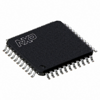
P89CV51RD2FBC,557 NXP Semiconductors, P89CV51RD2FBC,557 Datasheet - Page 41

P89CV51RD2FBC,557
Manufacturer Part Number
P89CV51RD2FBC,557
Description
IC 80C51 MCU FLASH 64K 44-TQFP
Manufacturer
NXP Semiconductors
Series
89Cr
Datasheet
1.P89CV51RB2FA512.pdf
(76 pages)
Specifications of P89CV51RD2FBC,557
Core Processor
8051
Core Size
8-Bit
Speed
40MHz
Connectivity
EBI/EMI, SPI, UART/USART
Peripherals
POR, PWM, WDT
Number Of I /o
32
Program Memory Size
64KB (64K x 8)
Program Memory Type
FLASH
Ram Size
1K x 8
Voltage - Supply (vcc/vdd)
4.5 V ~ 5.5 V
Oscillator Type
Internal
Operating Temperature
-40°C ~ 85°C
Package / Case
44-TQFP, 44-VQFP
Processor Series
P89CV5x
Core
80C51
Data Bus Width
8 bit
Data Ram Size
1 KB
Interface Type
SPI, UART
Maximum Clock Frequency
40 MHz
Number Of Programmable I/os
32
Number Of Timers
3
Operating Supply Voltage
4.5 V to 5.5 V
Maximum Operating Temperature
+ 85 C
Mounting Style
SMD/SMT
3rd Party Development Tools
PK51, CA51, A51, ULINK2
Minimum Operating Temperature
- 40 C
Cpu Family
89C
Device Core
80C51
Device Core Size
8b
Frequency (max)
40MHz
Total Internal Ram Size
1KB
# I/os (max)
32
Number Of Timers - General Purpose
3
Operating Supply Voltage (typ)
5V
Operating Supply Voltage (max)
5.5V
Operating Supply Voltage (min)
4.5V
Instruction Set Architecture
CISC
Operating Temp Range
-40C to 85C
Operating Temperature Classification
Industrial
Mounting
Surface Mount
Pin Count
44
Package Type
TQFP
Lead Free Status / RoHS Status
Lead free / RoHS Compliant
Eeprom Size
-
Data Converters
-
Lead Free Status / Rohs Status
Details
Other names
568-4257
935284103557
P89CV51RD2FBC
935284103557
P89CV51RD2FBC
Available stocks
Company
Part Number
Manufacturer
Quantity
Price
Company:
Part Number:
P89CV51RD2FBC,557
Manufacturer:
NXP Semiconductors
Quantity:
10 000
NXP Semiconductors
P89CV51RB2_RC2_RD2_3
Product data sheet
6.7.1 SPI features
6.7.2 SPI description
6.7 Serial Peripheral Interface (SPI)
address of all don’t cares. This effectively disables the automatic addressing mode and
allows the microcontroller to use standard UART drivers which do not make use of this
feature.
The serial peripheral interface allows high-speed synchronous data transfer between the
P89CV51RB2/RC2/RD2 and peripheral devices or between several
P89CV51RB2/RC2/RD2 devices.
and slave SPI devices. The SPICLK pin is the clock output and input for the Master and
Slave modes, respectively. The SPI clock generator will start following a write to the
master devices SPI data register. The written data is then shifted out of the MOSI pin of
the master device into the MOSI pin of the slave device. Following a complete
transmission of one byte of data, the SPI clock generator is stopped and the SPI interrupt
Flag (SPIF) is set. An SPI interrupt request will be generated if the SPI Interrupt Enable bit
(SPIE) and the SPI interrupt enable bit, ES, are both set.
An external master drives the Slave Select input pin (SS) LOW to select the SPI module
as a slave. If SS has not been driven LOW, then the slave SPI unit is not active and the
MOSI pin can also be used as an input port pin.
CPHA and CPOL control the phase and polarity of the SPI clock (SCK).
Figure 18
•
•
•
•
•
•
•
Master or slave operation
10 MHz bit frequency (max)
LSB first or MSB first data transfer
Four programmable bit rates
End of transmission (SPIF)
Write-collision flag protection (WCOL)
Wake-up from Idle mode (Slave mode only)
show the four possible combinations of these two bits.
Rev. 03 — 25 August 2009
Figure 16
P89CV51RB2/RC2/RD2
shows the correspondence between master
80C51 with 1 kB RAM, SPI
© NXP B.V. 2009. All rights reserved.
Figure 17
and
41 of 76


