LPC3180FEL320,551 NXP Semiconductors, LPC3180FEL320,551 Datasheet
LPC3180FEL320,551
Specifications of LPC3180FEL320,551
LPC3180FEL320-S
LPC3180FEL320-S
Available stocks


Related parts for LPC3180FEL320,551


LPC3180FEL320,551 Summary of contents
Page 1
LPC3180 16/32-bit ARM microcontroller; hardware floating-point coprocessor, USB On-The-Go, and SDRAM memory interface Rev. 02 — 15 February 2007 1. General description The LPC3180 is an ARM9-based microcontroller for embedded applications requiring high performance combined with low power dissipation. It ...
Page 2
... NXP Semiconductors GPI, GPO, and GPIO pins. Includes 12 GPI pins, 24 GPO pins, and six GPIO pins. I 10-bit ADC with input multiplexing from three pins. I Real-Time Clock (RTC) with separate power supply and power domain, clocked by a dedicated 32 kHz oscillator. Includes a 128 byte scratch pad memory. The RTC may remain active when the rest of the chip is not powered ...
Page 3
... NXP Semiconductors 4. Block diagram VFP9 ETB ETM9 D-TCM I-TCM ARM 9EJS D-CACHE I-CACHE I-SIDE D-SIDE MMU CTRL CTRL DATA INSTR master layer 0 1 slave port 0 slave port 1 slave port 2 slave port 3 slave port 5 slave port 6 slave port 7 32 bit, 104 MHz ...
Page 4
... NXP Semiconductors 5. Pinning information 5.1 Pinning Fig 2. LPC3180 package Table 2. Pin allocation table Pin Symbol Pin Row A 1 U6_IRRX/ 2 PIO_INP[21] 5 JTAG1_TMS 6 9 VSS 10 13 RTCX_OUT 14 17 VDD28 18 21 VDD12 22 Row B 1 KEY_COL5 2 5 JTAG1_TCK 6 9 U1_RX/PIO_INP[15 VSS_RTCCORE 14 [ VSS_OSC 22 Row C ...
Page 5
... NXP Semiconductors Table 2. Pin allocation table Pin Symbol Pin 9 VSS 10 13 VSS_RTCOSC 14 17 VDD28 18 21 PLL397_LOOP 22 Row D 1 KEY_ROW4 2 5 U6_IRTX 6 9 U2_TX 10 13 RESET_N 14 17 VSS 18 [1] 21 i.c. 22 Row E 1 KEY_ROW2 2 21 VDD_AD28 22 Row F 1 VSS_IO28_02 2 21 RAM_D[29]/ 22 PIO_SD[10] Row G ...
Page 6
... NXP Semiconductors Table 2. Pin allocation table Pin Symbol Pin Row M 1 GPO_08 2 21 VSS_SDRAM_04 22 Row N 1 GPO_13 2 21 RAM_D[07] 22 Row P 1 GPO_18 2 21 RAM_D[04] 22 Row R 1 GPIO_01 2 21 VSS_CORE_06 22 Row T 1 GPIO_03/ 2 KEY_ROW7 21 RAM_CLKIN 22 Row U [ RAM_RAS_N 22 Row V 1 SPI1_DATIN ...
Page 7
... NXP Semiconductors Table 2. Pin allocation table Pin Symbol Pin 9 GPO_00/TST_CLK1 10 [ VSS_CORE_09 18 21 VSS_SDRAM_09 22 Row AC 1 I2C1_SDA 2 5 VSS 6 9 GPO_01 10 [ FLASH_IO[06 FLASH_CE_N 22 Row AD 1 VSS 2 5 VSS 6 9 GPO_14 10 [ FLASH_WR_N 18 21 FLASH_IO[00] 22 [1] These pins are connected internally and must be left unconnected in an application. ...
Page 8
... NXP Semiconductors 5.2 Pin description Table 3. Pin description Symbol Pin ADIN0 C24 ADIN1 E22 ADIN2 D23 FLASH_ALE AA16 FLASH_CE_N AC21 FLASH_CLE AC15 FLASH_IO[07:00] AD18, AC17, AD19, AB19, AC20, AC19, AD20, AD21 FLASH_RD_N AA17 FLASH_RDY AC18 FLASH_WR_N AD17 GPI_00 H1 GPI_01/ K3 SERVICE_N GPI_02 ...
Page 9
... NXP Semiconductors Table 3. Pin description …continued Symbol Pin GPO_00/ AB9 TST_CLK1 GPO_01 AC9 GPO_02 L4 GPO_03 L1 GPO_04 Y3 GPO_05 AB10 GPO_06 M4 GPO_07 M3 GPO_08 M1 GPO_09 N4 GPO_10 M2 GPO_11 AB1 GPO_12 P3 GPO_13 N1 GPO_14 AD9 GPO_15 R4 GPO_16 N2 GPO_17 B12 GPO_18 P1 GPO_19 AC10 GPO_20 AD10 GPO_21/ P4 U4_TX GPO_22/ ...
Page 10
... NXP Semiconductors Table 3. Pin description …continued Symbol Pin KEY_COL0 to D2, F4, C1, C2, E4, KEY_COL5 B1 KEY_ROW0 to G3, F2, E1, F3, D1, KEY_ROW5 E2 MS_BS Y1 MS_DIO0 to MS_DIO3 W2, U2, Y2, V4 MS_SCLK AA1 ONSW D12 PLL397_LOOP C21 PWM_OUT1 J2 PWM_OUT2 H3 RAM_A[14:00] W21, AA24, Y23, AB24, Y22, AA23, AB23, AB22, AC23, ...
Page 11
... NXP Semiconductors Table 3. Pin description …continued Symbol Pin SPI1_CLK W3 SPI1_DATIN V1 SPI1_DATIO W1 SPI2_CLK V3 SPI2_DATIN T4 SPI2_DATIO V2 SYSCLKEN C5 SYSX_IN A23 SYSX_OUT B23 TEST D3 TST_CLK2 AB3 U1_RX/ B9 PIO_INP[15] U1_TX B10 U2_HCTS/ B8 PIO_INP[16] U2_RX/ C7 PIO_INP[17] U2_TX D9 U3_RX/ C6 PIO_INP[18] U3_TX A7 U5_RX/PIO_INP[20] A2 U5_TX C4 U6_IRRX/ A1 PIO_INP[21] U6_IRTX D5 U7_HCTS/ B2 PIO_INP[22] ...
Page 12
... NXP Semiconductors Table 3. Pin description …continued Symbol Pin USB_DAT_VP/ AA8 U5_RX USB_I2C_SCL AC8 USB_I2C_SDA AD7 USB_OE_TP_N AD6 USB_SE0_VM/ AB7 U5_TX VDD12 B14, A21, B19 VDD_AD28 D24, E21 VDD_CORE12_01 to AA2, D6, K21, L3, VDD_CORE12_03, AA12, AB6, AB18 VDD_CORE12_05 to VDD_CORE12_08 VDD_COREFXD12_01, C10, D18 VDD_COREFXD12_02 VDD1828, ...
Page 13
... NXP Semiconductors Table 3. Pin description …continued Symbol Pin VSS_CORE_01 to C20, D8, D16, J4, VSS_CORE_09 R3, R21, AA5, AA10, AB17 VSS_IO1828_01 to D4, A10 VSS_IO1828_02 VSS_IO18_01 to AC16, AD15, AC12, VSS_IO18_04 AB8 VSS_IO28_01 to E3, F1, N3 VSS_IO28_03 VSS_OSC B21 VSS_PLL397 C23 VSS_PLLHCLK D19 VSS_PLLUSB B20 VSS_RTCCORE B13 VSS_RTCOSC ...
Page 14
... NXP Semiconductors 6. Functional description 6.1 Architectural overview The microcontroller is a general purpose 32-bit microprocessor, which offers high performance and very low power consumption. The ARM architecture is based on RISC principles, and the instruction set and related decode mechanism are much simpler than those of microprogrammed CISCs ...
Page 15
... NXP Semiconductors 6.3 AHB matrix The microcontroller has a multi-layer AHB matrix for inter-block communication. AHB is the ARM high-speed bus, which is part of the ARM bus architecture. AHB is a high-bandwidth low-latency bus that supports multi-master arbitration and a bus grant/request mechanism. For systems where there is only one bus master (the CPU), or ...
Page 16
... NXP Semiconductors off-chip SDRAM peripherals on AHB matrix slave port 7 peripherals on AHB matrix slave port 6 peripherals on AHB matrix slave port 5 on-chip memory Fig 3. LPC3180 memory map 6.6 SDRAM memory controller The SDRAM memory controller provides an interface between the system bus and external (off-chip) memory devices. A single chip select is supplied, supporting one group of SDRAM in the same address range ...
Page 17
... NXP Semiconductors devices of 64/128/256/512/1024 Mbit in size, as well as DDR SDRAM devices of 64/128/256/512/1024 Mbit in size. The SDRAM controller uses four data ports to allow simultaneous requests from multiple on-chip AHB bus masters. 6.7 NAND flash controllers The LPC3180 includes two NAND flash controllers, one for multi-level NAND flash devices and one for single-level NAND fl ...
Page 18
... NXP Semiconductors status and masked interrupt status registers allow versatile condition evaluation. In addition to peripheral functions, each of the six general purpose input/output pins and 12 general purpose input pins are connected directly to the interrupt controller. 6.10 General purpose parallel I/O Some device pins that are not dedicated to a specific peripheral function have been designed to be general purpose inputs, outputs, or I/Os. Also, some pins may be confi ...
Page 19
... NXP Semiconductors • Uses 32 kHz RTC clock 6.12 USB interface The LPC3180 supports USB in either device, host, or OTG configuration. 6.12.1 USB device controller The USB device controller enables 12 Mbit/s data exchange with a USB host controller. It consists of register interface, serial interface engine, endpoint buffer memory and DMA controller ...
Page 20
... NXP Semiconductors 6.12.3 USB OTG Controller USB OTG (On-The-Go supplement to the USB 2.0 specification that augments the capability of existing mobile devices and USB peripherals by adding host functionality for connection to USB peripherals. 6.12.3.1 Features • Fully compliant with On-The-Go supplement to the USB Specification 2.0 Revision 1.0. • ...
Page 21
... NXP Semiconductors 6.13.2.1 Features • Each high-speed UART has 64 byte Receive and Transmit FIFOs. • Receiver FIFO trigger points and 48 B. • Transmitter FIFO trigger points and 8 B. • Each high-speed UART has an internal baud rate generator. • The high-speed UARTs are designed to support data rates of (2400, 4800, 9600, 19200, 38400, 57600, 115200, 230400, 460800, 921600) bit/s. • ...
Page 22
... NXP Semiconductors • Busy input function. • DMA time out interrupt to allow detection of end of reception when using DMA. • Timed interrupt to facilitate emptying the FIFO at the end of a transmission. • SPI clock and data pins may be used as general purpose pins if the SPI is not used. ...
Page 23
... NXP Semiconductors • Counter or Timer operation. • Two 32-bit capture registers. • Three 32-bit match registers that allow: – Continuous operation with optional interrupt generation on match. – Stop timer on match with optional interrupt generation. – Reset timer on match with optional interrupt generation. ...
Page 24
... NXP Semiconductors 6.21 RTC The RTC runs at 32768 Hz using a very low power oscillator. The RTC counts seconds and can generate alarm interrupts that can wake up the device from Stop mode. The RTCCLK can also clock the 397x PLL, the Millisecond Timer, the ADC, the Keyboard Scanner and the PWMs ...
Page 25
... NXP Semiconductors 6.23 Reset Reset is accomplished by an active low signal on the RESET_N input pin. A reset pulse with a minimum width of 10 main oscillator clocks after the oscillator is stable is required to guarantee a valid chip reset. At power-up, 10 milliseconds should be allowed for the oscillator to start up and stabilize after V with a minimum duration of 10 clock pulses will also be applied if the watchdog timer generates an internal device reset ...
Page 26
... NXP Semiconductors At the PLL output, there is a post-divider that can be used to bring the CCO frequency down to the desired PLL output frequency. The post-divider value ‘P’, can divide the CCO output 16. The post-divider can also be bypassed, allowing the PLL CCO output to be used directly. The maximum PLL output frequency that is supported by the CPU is 208 MHz ...
Page 27
... NXP Semiconductors The ARM core has a Debug Communication Channel function built-in. The debug communication channel allows a program running on the target to communicate with the host debugger or another separate host without stopping the program flow or entering the debug state. 6.25.2 Embedded trace buffer The Embedded Trace Module (ETM) is connected directly to the ARM core ...
Page 28
... NXP Semiconductors 7. Limiting values Table 4. Limiting values In accordance with the Absolute Maximum Rating System (IEC 60134). Symbol Parameter V supply voltage (1.2 V) DD(1V2) V supply voltage (1.8 V) DD(1V8) V supply voltage (3.0 V) DD(3V0) V analog supply voltage (3.0 V) DDA(3V0) V supply voltage DD V analog input voltage ...
Page 29
... NXP Semiconductors 8. Static characteristics Table 5. Static characteristics +85 C, unless otherwise specified. a Symbol Parameter V supply voltage (1.2 V) DD(1V2) V supply voltage (1.8 V) DD(1V8) V supply voltage (3.0 V) DD(3V0) V analog supply voltage (3.0 V) DDA(3V0) V supply voltage DD I LOW-state input current IL I HIGH-state input current ...
Page 30
... NXP Semiconductors Table 5. Static characteristics +85 C, unless otherwise specified. a Symbol Parameter I Run mode supply current DD(run) I direct Run mode supply current DD(drun) I Stop mode supply current DD(stop) [1] Typical ratings are not guaranteed. The values listed are at room temperature (+25 C), nominal supply voltages. ...
Page 31
... NXP Semiconductors 9. Dynamic characteristics Table 6. Dynamic characteristics +85 C, unless otherwise specified. a Symbol Parameter External clock f external clock frequency ext Port pins t rise time r t fall time f [1] Parameters are valid over operating temperature range unless otherwise specified. [2] Supplied by an external crystal. ...
Page 32
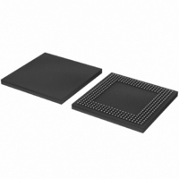
... NXP Semiconductors 10. Package outline LFBGA320: plastic low profile fine-pitch ball grid array package; 320 balls; body 0.9 mm ball A1 index area ball index area DIMENSIONS (mm are the original dimensions) A UNIT max. 0.3 1.0 0.35 mm 1.3 0.2 0.8 0.25 OUTLINE VERSION IEC SOT824-1 Fig 4 ...
Page 33
... NXP Semiconductors 11. Abbreviations Table 7. Acronym ADC AHB APB CISC DDR DMA DSP FAB FIFO FIQ GPI GPIO GPO IRQ MAC MMU OHCI OTG PLL PWM RC SDR SPI UART LPC3180_2 Preliminary data sheet 16/32-bit ARM microcontroller with external memory interface Abbreviations Description ...
Page 34
... Data sheet status Preliminary data sheet The format of this data sheet has been redesigned to comply with the new identity guidelines of NXP Semiconductors. Legal texts have been adapted to the new company name where appropriate. Table 4 “Limiting values”; updated <tbd> values for V Preliminary data sheet Rev. 02 — ...
Page 35
... For detailed and full information see the relevant full data sheet, which is available on request via the local NXP Semiconductors sales office. In case of any inconsistency or conflict with the short data sheet, the full data sheet shall prevail ...
Page 36
... NXP Semiconductors 15. Contents 1 General description . . . . . . . . . . . . . . . . . . . . . . 1 2 Features . . . . . . . . . . . . . . . . . . . . . . . . . . . . . . . 1 2.1 Key features . . . . . . . . . . . . . . . . . . . . . . . . . . . 1 3 Ordering information . . . . . . . . . . . . . . . . . . . . . 2 4 Block diagram . . . . . . . . . . . . . . . . . . . . . . . . . . 3 5 Pinning information . . . . . . . . . . . . . . . . . . . . . . 4 5.1 Pinning . . . . . . . . . . . . . . . . . . . . . . . . . . . . . . . 4 5.2 Pin description . . . . . . . . . . . . . . . . . . . . . . . . . 8 6 Functional description . . . . . . . . . . . . . . . . . . 14 6.1 Architectural overview 6.2 Vector Floating Point (VFP) coprocessor . . . . 14 6.3 AHB matrix . . . . . . . . . . . . . . . . . . . . . . . . . . . 15 6.4 On-chip SRAM . . . . . . . . . . . . . . . . . . . . . . . . 15 6 ...