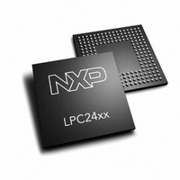
LPC2468FET208,551 NXP Semiconductors, LPC2468FET208,551 Datasheet - Page 37

LPC2468FET208,551
Manufacturer Part Number
LPC2468FET208,551
Description
IC ARM7 MCU FLASH 512K 208TFBGA
Manufacturer
NXP Semiconductors
Series
LPC2400r
Specifications of LPC2468FET208,551
Program Memory Type
FLASH
Program Memory Size
512KB (512K x 8)
Package / Case
208-TFBGA
Core Processor
ARM7
Core Size
16/32-Bit
Speed
72MHz
Connectivity
CAN, EBI/EMI, Ethernet, I²C, Microwire, MMC, SPI, SSI, SSP, UART/USART, USB OTG
Peripherals
Brown-out Detect/Reset, DMA, I²S, POR, PWM, WDT
Number Of I /o
160
Ram Size
98K x 8
Voltage - Supply (vcc/vdd)
3 V ~ 3.6 V
Data Converters
A/D 8x10b; D/A 1x10b
Oscillator Type
Internal
Operating Temperature
-40°C ~ 85°C
Processor Series
LPC24
Core
ARM7TDMI-S
Data Bus Width
16 bit, 32 bit
Data Ram Size
98 KB
Interface Type
CAN/I2S/ISP/SSP/UART/USB
Maximum Clock Frequency
72 MHz
Number Of Programmable I/os
160
Number Of Timers
6
Operating Supply Voltage
3.3 V
Maximum Operating Temperature
+ 85 C
Mounting Style
SMD/SMT
3rd Party Development Tools
MDK-ARM, RL-ARM, ULINK2, IRD-LPC2468-DEV, SAB-TFBGA208, KSK-LPC2468-PL
Development Tools By Supplier
OM10100
Minimum Operating Temperature
- 40 C
On-chip Adc
8-ch x 10-bit
On-chip Dac
1-ch x 10-bit
Package
208TFBGA
Device Core
ARM7TDMI-S
Family Name
LPC2000
Maximum Speed
72 MHz
Lead Free Status / RoHS Status
Lead free / RoHS Compliant
For Use With
622-1025 - KIT DEV IND REF DESIGN LPC2468622-1024 - BOARD SCKT ADAPTER FOR TFBGA208568-4358 - DISPLAY QVGA TFT FOR OM10100568-4309 - BOARD EXTENSION LPCSTICK568-4308 - EVAL LPC-STICK WITH LPC2468MCB2400U - BOARD EVAL MCB2400 + ULINK2MCB2400 - BOARD EVAL FOR NXP LPC246X SER622-1005 - USB IN-CIRCUIT PROG ARM7 LPC2K
Eeprom Size
-
Lead Free Status / Rohs Status
Lead free / RoHS Compliant
Other names
568-4262
935283234551
LPC2468FET208-S
935283234551
LPC2468FET208-S
Available stocks
Company
Part Number
Manufacturer
Quantity
Price
Company:
Part Number:
LPC2468FET208,551
Manufacturer:
NXP
Quantity:
6 174
Company:
Part Number:
LPC2468FET208,551
Manufacturer:
NXP Semiconductors
Quantity:
10 000
NXP Semiconductors
LPC2468
Product data sheet
7.20.1 Features
7.21.1 Features
7.21 General purpose 32-bit timers/external event counters
The I
and one word select signal. The basic I
master, and one slave. The I
and receive channel, each of which can operate as either a master or a slave.
The LPC2468 includes four 32-bit Timer/Counters. The Timer/Counter is designed to
count cycles of the system derived clock or an externally-supplied clock. It can optionally
generate interrupts or perform other actions at specified timer values, based on four
match registers. The Timer/Counter also includes four capture inputs to trap the timer
value when an input signal transitions, optionally generating an interrupt.
•
•
•
•
•
•
•
•
•
•
•
•
•
•
The interface has separate input/output channels each of which can operate in master
or slave mode.
Capable of handling 8-bit, 16-bit, and 32-bit word sizes.
Mono and stereo audio data supported.
The sampling frequency can range from 16 kHz to 48 kHz (16, 22.05, 32, 44.1,
48) kHz.
Configurable word select period in master mode (separately for I
Two 8 word FIFO data buffers are provided, one for transmit and one for receive.
Generates interrupt requests when buffer levels cross a programmable boundary.
Two DMA requests, controlled by programmable buffer levels. These are connected
to the GPDMA block.
Controls include reset, stop and mute options separately for I
A 32-bit Timer/Counter with a programmable 32-bit prescaler.
Counter or Timer operation.
Up to four 32-bit capture channels per timer, that can take a snapshot of the timer
value when an input signal transitions. A capture event may also optionally generate
an interrupt.
Four 32-bit match registers that allow:
– Continuous operation with optional interrupt generation on match.
– Stop timer on match with optional interrupt generation.
– Reset timer on match with optional interrupt generation.
Up to four external outputs corresponding to match registers, with the following
capabilities:
– Set LOW on match.
– Set HIGH on match.
– Toggle on match.
– Do nothing on match.
2
S-bus specification defines a 3-wire serial bus using one data line, one clock line,
All information provided in this document is subject to legal disclaimers.
Rev. 5 — 15 October 2010
2
S interface on the LPC2468 provides a separate transmit
2
S connection has one master, which is always the
Single-chip 16-bit/32-bit micro
2
S input and I
2
S input and output).
LPC2468
© NXP B.V. 2010. All rights reserved.
2
S output.
37 of 85


