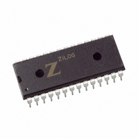
Z8F0823PJ005SG Zilog, Z8F0823PJ005SG Datasheet - Page 152

Z8F0823PJ005SG
Manufacturer Part Number
Z8F0823PJ005SG
Description
IC ENCORE MCU FLASH 8K 28-DIP
Manufacturer
Zilog
Series
Encore!® XP®r
Datasheet
1.Z8F0813PH005SC.pdf
(227 pages)
Specifications of Z8F0823PJ005SG
Core Processor
Z8
Core Size
8-Bit
Speed
5MHz
Connectivity
IrDA, UART/USART
Peripherals
Brown-out Detect/Reset, LED, POR, PWM, WDT
Number Of I /o
22
Program Memory Size
8KB (8K x 8)
Program Memory Type
FLASH
Ram Size
1K x 8
Voltage - Supply (vcc/vdd)
2.7 V ~ 3.6 V
Data Converters
A/D 8x10b
Oscillator Type
Internal
Operating Temperature
0°C ~ 70°C
Package / Case
28-DIP (0.600", 15.24mm)
Lead Free Status / RoHS Status
Lead free / RoHS Compliant
Eeprom Size
-
Other names
269-4218
Z8F0823PJ005SG
Z8F0823PJ005SG
- Current page: 152 of 227
- Download datasheet (3Mb)
BITS
FIELD
RESET
R/W
ADDR
Note: U = Unchanged by Reset. R/W = Read/Write.
PS025203-0405
Flash Program Memory Address 0000H
WDT_RES WDT_AO
R/W
U
7
WDT_RES—Watch-Dog Timer Reset
0 = Watch-Dog Timer time-out generates an interrupt request. Interrupts must be globally
enabled for the eZ8 CPU to acknowledge the interrupt request.
1 = Watch-Dog Timer time-out causes a system reset. This setting is the default for unpro-
grammed (erased) Flash.
WDT_AO—Watch-Dog Timer Always On
0 = Watch-Dog Timer is automatically enabled upon application of system power. Watch-
Dog Timer can not be disabled.
1 = Watch-Dog Timer is enabled upon execution of the WDT instruction. Once enabled,
the Watch-Dog Timer can only be disabled by a Reset or STOP Mode Recovery. This set-
ting is the default for unprogrammed (erased) Flash.
Reserved—Must be 1
VBO_AO—Voltage Brown-Out Protection Always On
0 = Voltage Brown-Out Protection is disabled in STOP mode to reduce total power con-
sumption.
1 = Voltage Brown-Out Protection is always enabled including during STOP mode. This
setting is the default for unprogrammed (erased) Flash.
FRP—Flash Read Protect
0 = User program code is inaccessible. Limited control features are available through the
On-Chip Debugger.
1 = User program code is accessible. All On-Chip Debugger commands are enabled. This
setting is the default for unprogrammed (erased) Flash.
Reserved—Must be 1.
FWP—Flash Write Protect
This Option Bit provides Flash Program Memory protection:
0 = Programming and erasure disabled for all of Flash Program Memory. Programming,
Page Erase, and Mass Erase through User Code is disabled. Mass Erase is available using
the On-Chip Debugger.
1 = Programming, Page Erase, and Mass Erase are enabled for all of Flash Program Mem-
ory.
Table 87. Flash Option Bits at Program Memory Address 0000H
R/W
U
6
R/W
U
5
Reserved
P R E L I M I N A R Y
Program Memory 0000H
R/W
U
4
VBO_AO
R/W
U
3
Z8 Encore!
FRP
R/W
U
2
Product Specification
Reserved
®
R/W
U
1
Z8F0823 Series
Flash Option Bits
FWP
R/W
U
0
135
Related parts for Z8F0823PJ005SG
Image
Part Number
Description
Manufacturer
Datasheet
Request
R

Part Number:
Description:
Communication Controllers, ZILOG INTELLIGENT PERIPHERAL CONTROLLER (ZIP)
Manufacturer:
Zilog, Inc.
Datasheet:

Part Number:
Description:
KIT DEV FOR Z8 ENCORE 16K TO 64K
Manufacturer:
Zilog
Datasheet:

Part Number:
Description:
KIT DEV Z8 ENCORE XP 28-PIN
Manufacturer:
Zilog
Datasheet:

Part Number:
Description:
DEV KIT FOR Z8 ENCORE 8K/4K
Manufacturer:
Zilog
Datasheet:

Part Number:
Description:
KIT DEV Z8 ENCORE XP 28-PIN
Manufacturer:
Zilog
Datasheet:

Part Number:
Description:
DEV KIT FOR Z8 ENCORE 4K TO 8K
Manufacturer:
Zilog
Datasheet:

Part Number:
Description:
CMOS Z8 microcontroller. ROM 16 Kbytes, RAM 256 bytes, speed 16 MHz, 32 lines I/O, 3.0V to 5.5V
Manufacturer:
Zilog, Inc.
Datasheet:

Part Number:
Description:
Low-cost microcontroller. 512 bytes ROM, 61 bytes RAM, 8 MHz
Manufacturer:
Zilog, Inc.
Datasheet:

Part Number:
Description:
Z8 4K OTP Microcontroller
Manufacturer:
Zilog, Inc.
Datasheet:

Part Number:
Description:
CMOS SUPER8 ROMLESS MCU
Manufacturer:
Zilog, Inc.
Datasheet:

Part Number:
Description:
SL1866 CMOSZ8 OTP Microcontroller
Manufacturer:
Zilog, Inc.
Datasheet:

Part Number:
Description:
SL1866 CMOSZ8 OTP Microcontroller
Manufacturer:
Zilog, Inc.
Datasheet:

Part Number:
Description:
OTP (KB) = 1, RAM = 125, Speed = 12, I/O = 14, 8-bit Timers = 2, Comm Interfaces Other Features = Por, LV Protect, Voltage = 4.5-5.5V
Manufacturer:
Zilog, Inc.
Datasheet:

Part Number:
Description:
Manufacturer:
Zilog, Inc.
Datasheet:


