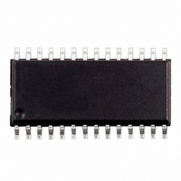
ST72C215G2M6 STMicroelectronics, ST72C215G2M6 Datasheet - Page 101

ST72C215G2M6
Manufacturer Part Number
ST72C215G2M6
Description
IC MCU 8BIT 8K FLASH SOIC-28
Manufacturer
STMicroelectronics
Series
ST7r
Datasheets
1.INDART-ST72C254.pdf
(3 pages)
2.ST72C104G1M6.pdf
(141 pages)
3.ST72C215G2M6.pdf
(140 pages)
Specifications of ST72C215G2M6
Core Processor
ST7
Core Size
8-Bit
Speed
16MHz
Connectivity
SPI
Peripherals
LVD, POR, PWM, WDT
Number Of I /o
22
Program Memory Size
8KB (8K x 8)
Program Memory Type
FLASH
Ram Size
256 x 8
Voltage - Supply (vcc/vdd)
3.2 V ~ 5.5 V
Data Converters
A/D 6x8b
Oscillator Type
Internal
Operating Temperature
-40°C ~ 85°C
Package / Case
28-SOIC (7.5mm Width)
Controller Family/series
ST7
No. Of I/o's
22
Ram Memory Size
256Byte
Cpu Speed
8MHz
No. Of Timers
2
Rohs Compliant
Yes
Processor Series
ST72C2x
Core
ST7
Data Bus Width
8 bit
Data Ram Size
256 B
Interface Type
SPI
Maximum Clock Frequency
16 MHz
Number Of Programmable I/os
22
Number Of Timers
3 bit
Operating Supply Voltage
3.2 V to 5.5 V
Maximum Operating Temperature
+ 85 C
Mounting Style
SMD/SMT
Development Tools By Supplier
ST7MDT1-DVP2/US
Minimum Operating Temperature
- 40 C
On-chip Adc
8 bit
Lead Free Status / RoHS Status
Lead free / RoHS Compliant
Eeprom Size
-
Lead Free Status / Rohs Status
In Transition
Available stocks
Company
Part Number
Manufacturer
Quantity
Price
Company:
Part Number:
ST72C215G2M6
Manufacturer:
ST
Quantity:
2 355
Part Number:
ST72C215G2M6
Manufacturer:
ST
Quantity:
20 000
FUNCTIONAL OPERATING CONDITIONS (Cont’d)
Figure 56. High LVD Threshold Versus V
Figure 57. Medium LVD Threshold Versus V
Figure 58. Low LVD Threshold Versus V
Notes:
1. LVD typical data are based on T
2. The minimum V
3. If the low LVD threshold is selected, when V
under reset.
DEVICE UNDER
DEVICE UNDER
DEVICE UNDER
IN THIS AREA
IN THIS AREA
IN THIS AREA
RESET
RESET
RESET
DD
f
f
f
OSC
OSC
OSC
rise time rate is needed to insure a correct device power-on and LVD reset. Not tested in production.
16
16
16
8
0
8
0
8
0
[MHz]
[MHz]
[MHz]
2.5
2.5
2.5
V
IT-
A
=25°C. They are given only as design guidelines and are not tested.
3
3
≥
3.00V
V
IT-
3.5
3.5
≥
DD
3.5V
DD
DD
V
falls below 3.2V, the device is guaranteed to be either functioning or
IT-
ST72104Gx, ST72215Gx, ST72216Gx, ST72254Gx
and f
and f
≥3.85
DD
and f
OSC
OSC
4
4
4
OSC
for ROM devices
for ROM devices
for ROM devices
4.5
4.5
4.5
5
5
5
2)3)
2)
2)
5.5
5.5
5.5
SUPPLY VOLTAGE [V]
SUPPLY VOLTAGE [V]
SUPPLY VOLTAGE [V]
FUNCTIONAL AREA
FUNCTIONAL AREA
FUNCTIONAL AREA
FUNCTIONALITY
NOT GUARANTEED
IN THIS AREA
FUNCTIONALITY
NOT GUARANTEED
IN THIS AREA
FUNCTIONALITY
NOT GUARANTEED
IN THIS AREA
101/141


