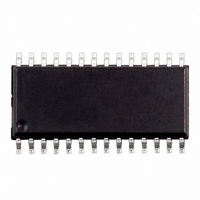
ST72C215G2M6 STMicroelectronics, ST72C215G2M6 Datasheet - Page 71

ST72C215G2M6
Manufacturer Part Number
ST72C215G2M6
Description
IC MCU 8BIT 8K FLASH SOIC-28
Manufacturer
STMicroelectronics
Series
ST7r
Datasheets
1.INDART-ST72C254.pdf
(3 pages)
2.ST72C104G1M6.pdf
(141 pages)
3.ST72C215G2M6.pdf
(140 pages)
Specifications of ST72C215G2M6
Core Processor
ST7
Core Size
8-Bit
Speed
16MHz
Connectivity
SPI
Peripherals
LVD, POR, PWM, WDT
Number Of I /o
22
Program Memory Size
8KB (8K x 8)
Program Memory Type
FLASH
Ram Size
256 x 8
Voltage - Supply (vcc/vdd)
3.2 V ~ 5.5 V
Data Converters
A/D 6x8b
Oscillator Type
Internal
Operating Temperature
-40°C ~ 85°C
Package / Case
28-SOIC (7.5mm Width)
Controller Family/series
ST7
No. Of I/o's
22
Ram Memory Size
256Byte
Cpu Speed
8MHz
No. Of Timers
2
Rohs Compliant
Yes
Processor Series
ST72C2x
Core
ST7
Data Bus Width
8 bit
Data Ram Size
256 B
Interface Type
SPI
Maximum Clock Frequency
16 MHz
Number Of Programmable I/os
22
Number Of Timers
3 bit
Operating Supply Voltage
3.2 V to 5.5 V
Maximum Operating Temperature
+ 85 C
Mounting Style
SMD/SMT
Development Tools By Supplier
ST7MDT1-DVP2/US
Minimum Operating Temperature
- 40 C
On-chip Adc
8 bit
Lead Free Status / RoHS Status
Lead free / RoHS Compliant
Eeprom Size
-
Lead Free Status / Rohs Status
In Transition
Available stocks
Company
Part Number
Manufacturer
Quantity
Price
Company:
Part Number:
ST72C215G2M6
Manufacturer:
ST
Quantity:
2 355
Part Number:
ST72C215G2M6
Manufacturer:
ST
Quantity:
20 000
SERIAL PERIPHERAL INTERFACE (Cont’d)
STATUS REGISTER (SR)
Read Only
Reset Value: 0000 0000 (00h)
Bit 7 = SPIF Serial Peripheral data transfer flag.
This bit is set by hardware when a transfer has
been completed. An interrupt is generated if
SPIE=1 in the CR register. It is cleared by a soft-
ware sequence (an access to the SR register fol-
lowed by a read or write to the DR register).
0: Data transfer is in progress or has been ap-
1: Data transfer between the device and an exter-
Note: While the SPIF bit is set, all writes to the DR
register are inhibited.
Bit 6 = WCOL Write Collision status.
This bit is set by hardware when a write to the DR
register is done during a transmit sequence. It is
cleared by a software sequence (see
0: No write collision occurred
1: A write collision has been detected
Bit 5 = Unused.
Bit 4 = MODF Mode Fault flag.
This bit is set by hardware when the SS pin is
pulled low in master mode (see
Master Mode
erated if SPIE=1 in the CR register. This bit is
cleared by a software sequence (An access to the
SR register while MODF=1 followed by a write to
the CR register).
0: No master mode fault detected
1: A fault in master mode has been detected
Bits 3-0 = Unused.
SPIF
proved by a clearing sequence.
nal device has been completed.
7
WCOL
Fault). An SPI interrupt can be gen-
-
MODF
-
Section 0.1.4.5
-
Figure
-
5).
ST72104Gx, ST72215Gx, ST72216Gx, ST72254Gx
0
-
DATA I/O REGISTER (DR)
Read/Write
Reset Value: Undefined
The DR register is used to transmit and receive
data on the serial bus. In the master device only a
write to this register will initiate transmission/re-
ception of another byte.
Notes: During the last clock cycle the SPIF bit is
set, a copy of the received data byte in the shift
register is moved to a buffer. When the user reads
the serial peripheral data I/O register, the buffer is
actually being read.
Warning:
A write to the DR register places data directly into
the shift register for transmission.
A read to the DR register returns the value located
in the buffer and not the contents of the shift regis-
ter (See
D7
7
D6
Figure
D5
2).
D4
D3
D2
D1
71/141
D0
0


