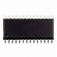
ST72C215G2M6 STMicroelectronics, ST72C215G2M6 Datasheet - Page 81

ST72C215G2M6
Manufacturer Part Number
ST72C215G2M6
Description
IC MCU 8BIT 8K FLASH SOIC-28
Manufacturer
STMicroelectronics
Series
ST7r
Datasheets
1.INDART-ST72C254.pdf
(3 pages)
2.ST72C104G1M6.pdf
(141 pages)
3.ST72C215G2M6.pdf
(140 pages)
Specifications of ST72C215G2M6
Core Processor
ST7
Core Size
8-Bit
Speed
16MHz
Connectivity
SPI
Peripherals
LVD, POR, PWM, WDT
Number Of I /o
22
Program Memory Size
8KB (8K x 8)
Program Memory Type
FLASH
Ram Size
256 x 8
Voltage - Supply (vcc/vdd)
3.2 V ~ 5.5 V
Data Converters
A/D 6x8b
Oscillator Type
Internal
Operating Temperature
-40°C ~ 85°C
Package / Case
28-SOIC (7.5mm Width)
Controller Family/series
ST7
No. Of I/o's
22
Ram Memory Size
256Byte
Cpu Speed
8MHz
No. Of Timers
2
Rohs Compliant
Yes
Processor Series
ST72C2x
Core
ST7
Data Bus Width
8 bit
Data Ram Size
256 B
Interface Type
SPI
Maximum Clock Frequency
16 MHz
Number Of Programmable I/os
22
Number Of Timers
3 bit
Operating Supply Voltage
3.2 V to 5.5 V
Maximum Operating Temperature
+ 85 C
Mounting Style
SMD/SMT
Development Tools By Supplier
ST7MDT1-DVP2/US
Minimum Operating Temperature
- 40 C
On-chip Adc
8 bit
Lead Free Status / RoHS Status
Lead free / RoHS Compliant
Eeprom Size
-
Lead Free Status / Rohs Status
In Transition
Available stocks
Company
Part Number
Manufacturer
Quantity
Price
Company:
Part Number:
ST72C215G2M6
Manufacturer:
ST
Quantity:
2 355
Part Number:
ST72C215G2M6
Manufacturer:
ST
Quantity:
20 000
I
I
Read Only
Reset Value: 0000 0000 (00h)
Bit 7 = EVF Event flag.
This bit is set by hardware as soon as an event oc-
curs. It is cleared by software reading SR2 register
in case of error event or as described in
is also cleared by hardware when the interface is
disabled (PE=0).
0: No event
1: One of the following events has occurred:
Bit 6 = ADD10 10-bit addressing in Master mode.
This bit is set by hardware when the master has
sent the first byte in 10-bit address mode. It is
cleared by software reading SR2 register followed
by a write in the DR register of the second address
byte. It is also cleared by hardware when the pe-
ripheral is disabled (PE=0).
0: No ADD10 event occurred.
1: Master has sent first address byte (header)
Bit 5 = TRA Transmitter/Receiver.
When BTF is set, TRA=1 if a data byte has been
transmitted. It is cleared automatically when BTF
is cleared. It is also cleared by hardware after de-
2
2
EVF
C BUS INTERFACE (Cont’d)
C STATUS REGISTER 1 (SR1)
– BTF=1 (Byte received or transmitted)
– ADSL=1 (Address matched in Slave mode
– SB=1 (Start condition generated in Master
– AF=1 (No acknowledge received after byte
– STOPF=1 (Stop condition detected in Slave
– ARLO=1 (Arbitration lost in Master mode)
– BERR=1 (Bus error, misplaced Start or Stop
– ADD10=1 (Master has sent header byte)
– Address byte successfully transmitted in Mas-
7
while ACK=1)
mode)
transmission)
mode)
condition detected)
ter mode.
ADD10
TRA
BUSY
BTF
ADSL
M/SL
Figure
ST72104Gx, ST72215Gx, ST72216Gx, ST72254Gx
SB
3. It
0
tection of Stop condition (STOPF=1), loss of bus
arbitration (ARLO=1) or when the interface is disa-
bled (PE=0).
0: Data byte received (if BTF=1)
1: Data byte transmitted
Bit 4 = BUSY Bus busy.
This bit is set by hardware on detection of a Start
condition and cleared by hardware on detection of
a Stop condition. It indicates a communication in
progress on the bus. The BUSY flag of the I2CSR1
register is cleared if a Bus Error occurs.
0: No communication on the bus
1: Communication ongoing on the bus
Bit 3 = BTF Byte transfer finished.
This bit is set by hardware as soon as a byte is cor-
rectly received or transmitted with interrupt gener-
ation if ITE=1. It is cleared by software reading
SR1 register followed by a read or write of DR reg-
ister. It is also cleared by hardware when the inter-
face is disabled (PE=0).
– Following a byte transmission, this bit is set after
– Following a byte reception, this bit is set after
The SCL line is held low while BTF=1.
0: Byte transfer not done
1: Byte transfer succeeded
Bit 2 = ADSL Address matched (Slave mode).
This bit is set by hardware as soon as the received
slave address matched with the OAR register con-
tent or a general call is recognized. An interrupt is
generated if ITE=1. It is cleared by software read-
ing SR1 register or by hardware when the inter-
face is disabled (PE=0).
The SCL line is held low while ADSL=1.
0: Address mismatched or not received
1: Received address matched
reception of the acknowledge clock pulse. In
case an address byte is sent, this bit is set only
after the EV6 event (See
cleared by reading SR1 register followed by writ-
ing the next byte in DR register.
transmission of the acknowledge clock pulse if
ACK=1. BTF is cleared by reading SR1 register
followed by reading the byte from DR register.
Figure
3). BTF is
81/141


