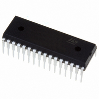
ST72F262G2B5 STMicroelectronics, ST72F262G2B5 Datasheet - Page 116

ST72F262G2B5
Manufacturer Part Number
ST72F262G2B5
Description
IC MCU 8BIT 8K FLASH 32-SDIP
Manufacturer
STMicroelectronics
Series
ST7r
Datasheet
1.STEVAL-ISQ002V1.pdf
(172 pages)
Specifications of ST72F262G2B5
Core Processor
ST7
Core Size
8-Bit
Speed
16MHz
Connectivity
SPI
Peripherals
LVD, POR, PWM, WDT
Number Of I /o
22
Program Memory Size
8KB (8K x 8)
Program Memory Type
FLASH
Ram Size
256 x 8
Voltage - Supply (vcc/vdd)
2.7 V ~ 5.5 V
Data Converters
A/D 6x10b
Oscillator Type
Internal
Operating Temperature
-10°C ~ 85°C
Package / Case
32-SDIP (0.400", 10.16mm)
Processor Series
ST72F2x
Core
ST7
Data Bus Width
8 bit
Data Ram Size
256 B
Interface Type
I2C, SCI, SPI
Maximum Clock Frequency
8 MHz
Number Of Programmable I/os
22
Number Of Timers
16 bit
Maximum Operating Temperature
+ 85 C
Mounting Style
Through Hole
Development Tools By Supplier
ST7F264-IND/USB, ST72F34X-SK/RAIS, ST7MDT10-DVP3, ST7MDT10-EMU3, STX-RLINK
Minimum Operating Temperature
- 40 C
On-chip Adc
8 bit
Lead Free Status / RoHS Status
Lead free / RoHS Compliant
Eeprom Size
-
Lead Free Status / Rohs Status
Details
Available stocks
Company
Part Number
Manufacturer
Quantity
Price
Company:
Part Number:
ST72F262G2B5
Manufacturer:
TAIYO
Quantity:
8 122
ST72260Gx, ST72262Gx, ST72264Gx
11.7 10-BIT A/D CONVERTER (ADC)
11.7.1 Introduction
The on-chip Analog to Digital Converter (ADC) pe-
ripheral is a 10-bit, successive approximation con-
verter with internal sample and hold circuitry. This
peripheral has 6 multiplexed analog input chan-
nels (refer to device pin out description) that allow
the peripheral to convert the analog voltage levels
from 6 different sources.
The result of the conversion is stored in a 10-bit
Data Register. The A/D converter is controlled
through a Control/Status Register.
11.7.2 Main Features
■
■
■
Figure 61. ADC Block Diagram
116/172
10-bit conversion
6 channels with multiplexed input
Linear successive approximation
AIN0
AINx
AIN1
f
CPU
ANALOG
MUX
EOC SPEED ADON SLOW
f
CPU,
3
ADCDRH
f
CPU
/2
,
f
CPU
ADCDRL
/4
D9
0
f
ADC
CH2
D8
■
■
■
The block diagram is shown in
11.7.3 Functional Description
11.7.3.1 Analog Power Supply
V
ence voltage pins. In some devices (refer to device
pin out description) they are internally connected
to the V
Conversion accuracy may therefore be impacted
by voltage drops and noise in the event of heavily
loaded or badly decoupled power supply lines.
CH1
D7
DDA
Data register (DR) which contains the results
Conversion complete status flag
On/off bit (to reduce consumption)
0
CH0
and V
D6
DD
0
and V
D5
ADCCSR
SSA
0
D4
are the high and low level refer-
SS
0
ANALOG TO DIGITAL
pins.
D3
CONVERTER
0
D2
0
Figure
D1
61.
D0


