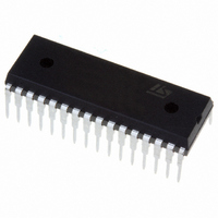
ST72F262G2B5 STMicroelectronics, ST72F262G2B5 Datasheet - Page 169

ST72F262G2B5
Manufacturer Part Number
ST72F262G2B5
Description
IC MCU 8BIT 8K FLASH 32-SDIP
Manufacturer
STMicroelectronics
Series
ST7r
Datasheet
1.STEVAL-ISQ002V1.pdf
(172 pages)
Specifications of ST72F262G2B5
Core Processor
ST7
Core Size
8-Bit
Speed
16MHz
Connectivity
SPI
Peripherals
LVD, POR, PWM, WDT
Number Of I /o
22
Program Memory Size
8KB (8K x 8)
Program Memory Type
FLASH
Ram Size
256 x 8
Voltage - Supply (vcc/vdd)
2.7 V ~ 5.5 V
Data Converters
A/D 6x10b
Oscillator Type
Internal
Operating Temperature
-10°C ~ 85°C
Package / Case
32-SDIP (0.400", 10.16mm)
Processor Series
ST72F2x
Core
ST7
Data Bus Width
8 bit
Data Ram Size
256 B
Interface Type
I2C, SCI, SPI
Maximum Clock Frequency
8 MHz
Number Of Programmable I/os
22
Number Of Timers
16 bit
Maximum Operating Temperature
+ 85 C
Mounting Style
Through Hole
Development Tools By Supplier
ST7F264-IND/USB, ST72F34X-SK/RAIS, ST7MDT10-DVP3, ST7MDT10-EMU3, STX-RLINK
Minimum Operating Temperature
- 40 C
On-chip Adc
8 bit
Lead Free Status / RoHS Status
Lead free / RoHS Compliant
Eeprom Size
-
Lead Free Status / Rohs Status
Details
Available stocks
Company
Part Number
Manufacturer
Quantity
Price
Company:
Part Number:
ST72F262G2B5
Manufacturer:
TAIYO
Quantity:
8 122
16.2.2 I/O Port B and C configuration
When using an external quartz crystal or ceramic
resonator, the f
cause the device goes into reserved mode control-
led by Port B and C.
This happens with either one of the following con-
figurations:
PB1=0, PC2=1, PB3=0 while PLL option is both
disabled and PC4 is toggling
PB1=0, PC2=1, PB3=0, PC4=1 while PLL option
is enabled
This is detailed in the following table:
As a consequence, for cycle-accurate operations,
these configurations are prohibited in either input
or output mode.
Workaround:
To avoid this occurring, it is recommended to con-
nect one of these pins to GND (PC2 or PC4) or
V
16.2.3 16-bit Timer PWM mode
After a write instruction to the OCiHR register, the
output compare function is inhibited until the
OCiLR register is also written.
16.2.4 SPI Multimaster Mode
Multi master mode is not supported.
16.2.5 Internal RC oscillator with LVD
If the LVD is disabled, the internal RC oscillator
clock source cannot be used.
In ICP mode, new flash devices must be pro-
grammed with an external clock connected to the
OSC1 pin or using a crystal or ceramic resonator.
In the STVP7 programming tool software, select
the “OPTIONS DISABLED” mode.
16.2.6 External clock with PLL
The PLL option is not supported for use with exter-
nal clock source.
16.2.7 Halt mode power consumption with ADC
on
If the A/D converter is being used when Halt mode
is entered, the power consumption in Halt Mode
may exceed the maximum specified in the datash-
eet.
PLL PB1 PC2 PB3 PC4 Clock Disturbance
OFF
DD
ON
(PB1 or PB3).
0
0
1
1
OSC2
0
0
clock may be disturbed be-
Tog
glin
g
1
Max. 2 clock cycles
lost at each rising or
falling edge of PC4
Max. 1 clock cycle
lost out of every 16
Workaround
Switch off the ADC by software (ADON=0) before
executing a HALT instruction.
16.2.8 Active Halt wake-up by external interrupt
External interrupts are not able to wake-up the
MCU from Active Halt mode. The MCU can only
exit from Active Halt mode by means of an MCC/
RTC interrupt or a reset.
Workaround
Use WAIT mode if external interrupt capability is
required in low power mode.
16.2.9 SCI Wrong Break duration
Description
A single break character is sent by setting and re-
setting the SBK bit in the SCICR2 register. In
some cases, the break character may have a long-
er duration than expected:
- 20 bits instead of 10 bits if M=0
- 22 bits instead of 11 bits if M=1.
In the same way, as long as the SBK bit is set,
break characters are sent to the TDO pin. This
may lead to generate one break more than expect-
ed.
Occurrence
The occurrence of the problem is random and pro-
portional to the baudrate. With a transmit frequen-
cy of 19200 baud (fCPU=8MHz and SCI-
BRR=0xC9), the wrong break duration occurrence
is around 1%.
Workaround
If this wrong duration is not compliant with the
communication protocol in the application, soft-
ware can request that an Idle line be generated
before the break character. In this case, the break
duration is always correct assuming the applica-
tion is not doing anything between the idle and the
break. This can be ensured by temporarily disa-
bling interrupts.
The exact sequence is:
16.2.10 A/D converter accuracy for first
conversion
When the ADC is enabled after being powered
down (for example when waking up from HALT,
ACTIVE-HALT or setting the ADON bit in the AD-
CCSR register), the first conversion (8-bit or 10-
– Disable interrupts
– Reset and Set TE (IDLE request)
– Set and Reset SBK (Break Request)
– Re-enable interrupts
ST72260Gx, ST72262Gx, ST72264Gx
169/172


