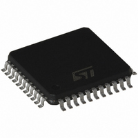
ST72F561J4T6 STMicroelectronics, ST72F561J4T6 Datasheet - Page 148

ST72F561J4T6
Manufacturer Part Number
ST72F561J4T6
Description
IC MCU 8BIT 16K FLASH 44-LQFP
Manufacturer
STMicroelectronics
Series
ST7r
Datasheet
1.ST72F561K6T6.pdf
(265 pages)
Specifications of ST72F561J4T6
Core Processor
ST7
Core Size
8-Bit
Speed
8MHz
Connectivity
CAN, LINSCI, SPI
Peripherals
LVD, POR, PWM, WDT
Number Of I /o
32
Program Memory Size
16KB (16K x 8)
Program Memory Type
FLASH
Ram Size
1K x 8
Voltage - Supply (vcc/vdd)
3.8 V ~ 5.5 V
Data Converters
A/D 16x10b
Oscillator Type
External
Operating Temperature
-40°C ~ 85°C
Package / Case
44-LQFP
Processor Series
ST72F5x
Core
ST7
Data Bus Width
8 bit
Data Ram Size
1 KB
Interface Type
CAN, SCI, SPI
Maximum Clock Frequency
8 MHz
Number Of Programmable I/os
48
Number Of Timers
3
Maximum Operating Temperature
+ 85 C
Mounting Style
SMD/SMT
Development Tools By Supplier
STX-RLINK
Minimum Operating Temperature
- 40 C
On-chip Adc
10 bit, 16 Channel
For Use With
497-8374 - BOARD DEVELOPMENT FOR ST72F561
Lead Free Status / RoHS Status
Lead free / RoHS Compliant
Eeprom Size
-
Lead Free Status / Rohs Status
Details
Available stocks
Company
Part Number
Manufacturer
Quantity
Price
Company:
Part Number:
ST72F561J4T6
Manufacturer:
COILCRAFT
Quantity:
4 000
Company:
Part Number:
ST72F561J4T6
Manufacturer:
STMicroelectronics
Quantity:
10 000
- Current page: 148 of 265
- Download datasheet (10Mb)
ST72561
LINSCI™ SERIAL COMMUNICATION INTERFACE (LIN Mode) (cont’d)
CONTROL REGISTER 2 (SCICR2)
Read/Write
Reset Value: 0000 0000 (00 h)
Bits 7:2 Same function as in SCI mode; please re-
fer to
tion.
Bit 1 = RWU Receiver wake-up.
This bit determines if the SCI is in mute mode or
not. It is set and cleared by software and can be
cleared by hardware when a wake-up sequence is
recognized.
0: Receiver in active mode
1: Receiver in mute mode
Notes:
– Mute mode is recommended for detecting only
– In LIN slave mode, when RDRF is set, the soft-
Bit 0 = SBK Send break.
This bit set is used to send break characters. It is
set and cleared by software.
0: No break character is transmitted
1: Break characters are transmitted
Note: If the SBK bit is set to “1” and then to “0”, the
transmitter will send a BREAK word at the end of
the current word.
CONTROL REGISTER 3 (SCICR3)
Read/Write
Reset Value: 0000 0000 (00h)
Bit 7 = LDUM LIN Divider Update Method.
This bit is set and cleared by software and is also
cleared by hardware (when RDRF = 1). It is only
used in LIN Slave mode. It determines how the LIN
Divider can be updated by software.
0: LDIV is updated as soon as LPR is written (if no
148/265
LDUM LINE
the Header and avoiding the reception of any
other characters. For more details, please refer
to
ware can not set or clear the RWU bit.
TIE
Auto Synchronization update occurs at the
same time).
7
7
Section 0.1.9.3 LIN
Section 0.1.8 SCI Mode Register Descrip-
TCIE
LSLV
RIE
LASE
ILIE
Reception.
LHDM
TE
RE
LHIE LHDF
RWU
SBK
LSF
0
0
1: LDIV is updated at the next received character
Notes:
- If no write to LPR is performed between the set-
ting of LDUM bit and the reception of the next
character, LDIV will be updated with the old value.
- After LDUM has been set, it is possible to reset
the LDUM bit by software. In this case, LDIV can
be modified by writing into LPR / LPFR registers.
Bits 6:5 = LINE, LSLV LIN Mode Enable Bits.
These bits configure the LIN mode:
The LIN Master configuration enables:
The capability to send LIN Synch Breaks (13 low
bits) using the SBK bit in the SCICR2 register.
The LIN Slave configuration enables:
Bit 4 = LASE LIN Auto Synch Enable.
This bit enables the Auto Synch Unit (ASU). It is
set and cleared by software. It is only usable in LIN
Slave mode.
0: Auto Synch Unit disabled
1: Auto Synch Unit enabled.
Bit 3 = LHDM LIN Header Detection Method
This bit is set and cleared by software. It is only us-
able in LIN Slave mode. It enables the Header De-
tection Method. In addition if the RWU bit in the
(when RDRF = 1) after a write to the LPR regis-
ter
– The LIN Slave Baud Rate generator. The LIN
– Management of LIN Headers.
– LIN Synch Break detection (11-bit dominant).
– LIN Wake-Up method (see LHDM bit) instead
– Inhibition of Break transmission capability
– LIN Parity Checking (in conjunction with the
LINE
Divider (LDIV) is then represented by the LPR
and LPFR registers. The LPR and LPFR reg-
isters are read/write accessible at the address
of the SCIBRR register and the address of the
SCIETPR register
of the normal SCI Wake-Up method.
(SBK has no effect)
PCE bit)
0
1
LSLV
x
0
1
LIN mode disabled
LIN Master Mode
LIN Slave Mode
Meaning
Related parts for ST72F561J4T6
Image
Part Number
Description
Manufacturer
Datasheet
Request
R

Part Number:
Description:
STMicroelectronics [RIPPLE-CARRY BINARY COUNTER/DIVIDERS]
Manufacturer:
STMicroelectronics
Datasheet:

Part Number:
Description:
STMicroelectronics [LIQUID-CRYSTAL DISPLAY DRIVERS]
Manufacturer:
STMicroelectronics
Datasheet:

Part Number:
Description:
BOARD EVAL FOR MEMS SENSORS
Manufacturer:
STMicroelectronics
Datasheet:

Part Number:
Description:
NPN TRANSISTOR POWER MODULE
Manufacturer:
STMicroelectronics
Datasheet:

Part Number:
Description:
TURBOSWITCH ULTRA-FAST HIGH VOLTAGE DIODE
Manufacturer:
STMicroelectronics
Datasheet:

Part Number:
Description:
Manufacturer:
STMicroelectronics
Datasheet:

Part Number:
Description:
DIODE / SCR MODULE
Manufacturer:
STMicroelectronics
Datasheet:

Part Number:
Description:
DIODE / SCR MODULE
Manufacturer:
STMicroelectronics
Datasheet:

Part Number:
Description:
Search -----> STE16N100
Manufacturer:
STMicroelectronics
Datasheet:

Part Number:
Description:
Search ---> STE53NA50
Manufacturer:
STMicroelectronics
Datasheet:

Part Number:
Description:
NPN Transistor Power Module
Manufacturer:
STMicroelectronics
Datasheet:

Part Number:
Description:
DIODE / SCR MODULE
Manufacturer:
STMicroelectronics
Datasheet:


